Terminologie (original) (raw)
Terminologie a n�kter� dal�� zkratky
Microwave MCM-D
MCM-D technology is well suited for high-frequency applications, particularly due to its high precision and possibility to integrate re-sistive and capacitive layers. Oriented towards integrating the whole front-end RF of wireless communications systems in one single package.
PWB, HD-PWB
podobn�: printed circuit board (PCB),
Neboli Printed Wiring Board, nebo dnes nov�j�� technologie prozaicky nazvan� High Density-PWB. Tato technologie vyu��v� jako podklad bud keramiku, nebo sklen�n�mi vl�kny vyztu�enou epoxydovou desti�ku. Dal�� v�vojov� krok by m�l b�t
"high-density flex, polyimide based technology", kter� vypad� asi n�sledovn�: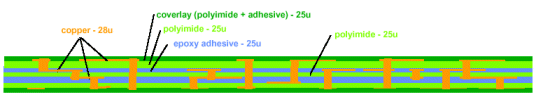
Tato desti�ka je asi 300um tlust�, cty�vrstv�. Z toho dv� vrstvy jsou pro sign�lov� cesty, izola�n� vrstva a vrchni vrstva pro mont� I/O.
Nev�hodou polyimid� byla n�chylnost k vlhnut�. V sou�astnosti se v�ak ji� poda�ilo tuto nev�hodu odstranit. Parametry: Nevratn� absorbce vody: 0.2%; dielektrick� konstanta: 2.8; nejmen�� tlou��ka vrstvy 5-10um.
Porovn�n� obvykl�ch technologi�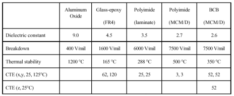
Known Good Die (KGD)
One of the key elements determining the success of miniaturized electronic systems is the availability of the necessary components in a tested bare die form (KGD) or mini-mally packaged components (chip scale package or CSP). Component availability, level of goodness, handling, shipping and storage, as well as design data, test and assembly are among the most urgent aspects to be addressed. In this field, IMEC is leading a European funded program, the GOOD-DIE Network, which has started its second phase of activities in November 1998. Results from the first phase include the commercial launch in May of the GOOD-DIE service, a component database tailored for the need of the MCM designer, providing high-level quality information on a large number of KGD and CSP devices (www.gooddie.com). In the second phase, the objec-tive of the network, now counting more than 600 members, is to increase the aware-ness of the need for KGD and CSP throughout the industry and to disseminate infor-mation related to KGD, CSP and HDPs. Another activity with CENELEC is to generate a European standard for the exchange of data on KGD and CSPs (P142, C266). More information on GOOD-DIE can be found at: www.imec.be/kgd The polymer stud grid array package (PSGA)
The PSGA is a novel packaging concept, jointly developed by IMEC and Siemens. The PSGA is an area array package which uses metallized plastic studs, moulded to the body of the package, instead of large solder balls as with ball grid array (BGA) pack-ages. This results in a more reliable and cost effective package. The nearly cylindrical studs have a higher aspect ratio (height -- diameter ratio) than the solder balls of BGA packages. This makes this package concept well suited for chip scale and chip sized packages with stud pitches of 0.8 to 0.5 mm (D3, P182, P183). The PSGA and the technology for realizing PSGA packages is now being commercial-ized worldwide by Siemens. IMEC works with Siemens on the further optimization and characterization of the package as well as on novel concepts for chip sized pack-ages with smaller pitches. In the last year, a 72 pin cavity-up PSGA package with 0.8 mm stud pitch was realized
BGA
Ball grid arrary