Computex 2012: ASRock's New Motherboards: X79 Extreme11 with LSI SAS and Z77 OC Formula (original) (raw)
ASRock have now gone slightly mad. You could argue that within that madness lies some semblance of innovation, as they are going to release a mad product with features that no-one else in the motherboard market is considering. Take their upcoming X79 Extreme11:
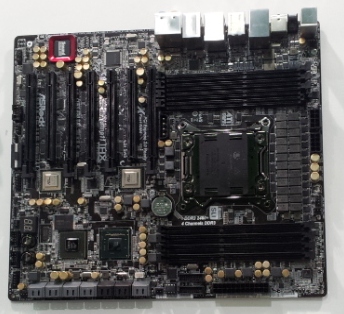
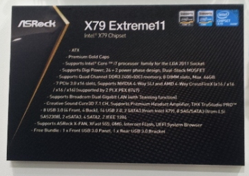
In case these pictures are in any way confusing, let's break it down. The X79 chipset comes with 40 PCIe lanes from the CPU, enough for x16/x8/x8/x8 when using four-way SLI or CrossFire. So what happens when ASRock add two PLX PXE 8747 chips? These chips typically take 16 PCIe 3.0 lanes and essentially switch them into 32, so ASRock are taking 32 lanes from the CPU and making them 64, allowing for x16/x16/x16/x16. The BOM cost for these chips are obviously a premium as well.
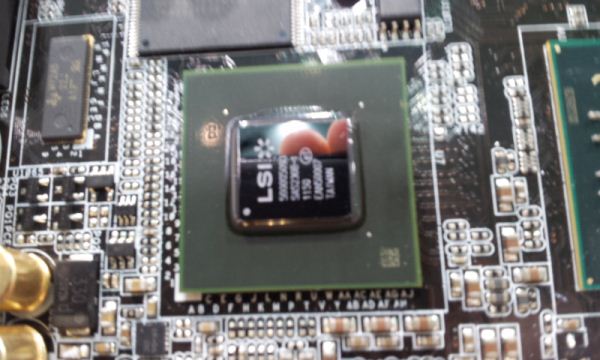
But 'that leaves 8 lanes' I hear you say. Well that leaves another X79 Extreme11 feature to discuss - the addition of an LSI chip.
The LSI chip enables 8 SAS ports on the motherboard, all capable of RAID (at least RAID 0). Hence why in the first picture you see a total of 14 SATA looking ports. ASRock believe that there is a market in users who will want to utilise the x16/x16/x16/x16 usage scenario, or the 8 SAS port one, or both.
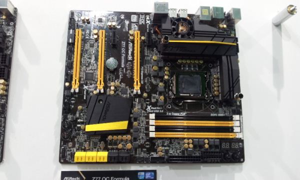
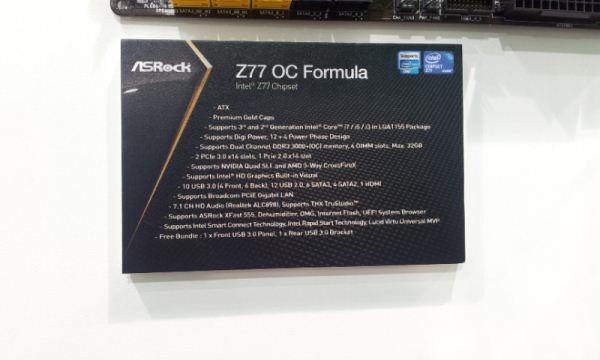
Also up for a look is a new direction for ASRock - serious overclocking. For a while now, top overclocker NickShih has been under the employ of ASRock for guidance on how to organise their systems to cater for normal and extreme overclocking. But for the first time, ASRock are releasing a motherboard specifically aimed at that crowd - the Z77 OC Formula:
The OC Formula has several features designed specifically for overclocking. The power delivery is very efficient, reportedly around 97% due to a dual-stack MOSFET and Silicon-Chromium chokes. The VRM heatsink is bulky with an additional fan, but is also a water block for water cooled systems. The CPU 12V power delivery uses solid pins for cleaner power delivery and can hold more current under load. As we look at the board above, just below the memory are a set of dual two-digit debug LEDs, which ASRock will program to display temperature (e.g. -130 under liquid nitrogen). Next to these LEDs are two sets of voltage read points, and +/- buttons for BCLK adjustments. The pins inside the socket are also thicker, to reduce resistance between the CPU and the motherboard.
Time will tell if this is a board worthy of overclocking world records, or if these features can help regular overclockers achieve good and stable systems.
