Understanding RAM Timings - Hardware Secrets (original) (raw)
RAM Speed
DDR, DDR2, and DDR3 RAM memories are classified according to the maximum speed at which they can work, as well as their timings. Random Access Memory Timings are numbers such as 3-4-4-8, 5-5-5-15, 7-7-7-21, or 9-9-9-24, the lower the better. In this tutorial, we will explain exactly what each one of these RAM Timings means.
DDR, DDR2, and DDR3 Ram memories follow the DDRxxx/PCyyyy classification. By the way, if you are interested in knowing the difference between DDR, DDR2, and DDR3 RAM memories, read our tutorial on this subject.
How to understand the RAM classifications?
The first classification
The first number, xxx, indicates the maximum clock speed that the memory chips support. For instance, DDR400 memories work at 400 MHz at the most, DDR2-800 can work up to 800 MHz, and DDR3-1333 can work up to 1,333 MHz. It is important to note that this is not the real clock speed of the memory. The real clock of the DDR, DDR2 and DDR3 memories is half of the labeled clock speed. Therefore DDR400 memories work at 200 MHz, DDR2-800 memories work at 400 MHz, and DDR3-1333 memories work at 666 MHz.
The second classification
The second number indicates the maximum transfer rate that the memory reaches, in MB/s. DDR400 memories transfer data at 3,200 MB/s at the most, and hence they are labeled as PC3200. DDR2-800 memories transfer data at 6,400 MB/s and they are labeled as PC2-6400. And DDR3-1333 memories can transfer data at 10,664 MB/s and they are labeled as PC3-10600 or PC3-10666. As you can see, we use the number “2” or “3” after “DDR” or “PC” to indicate that we are talking about a DDR2 or DDR3 memory, not DDR.
The first classification, DDRxxx, is the standard used to classify memory chips, while the second classification, PCyyyy, is the standard used to classify memory modules. In Figure 1, you can see a PC3-10666 memory module, which uses DDR3-1333 memory chips. Pay attention to the RAM timings (7-7-7-18) and voltage (1.5 V).
How to calculate the maximum transfer rate for a memory module?
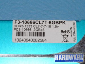
Figure 1: A DDR3-1333/PC3-10666 memory module
The maximum transfer rate for a memory module can be calculated through the following formula:
Maximum Theoretical Transfer Rate = clock x number of bits / 8
Since DIMM modules transfer 64 bits at a time, “number of bits” will be 64. As 64 / 8 equals 8, we can simplify this formula to:
Maximum Theoretical Transfer Rate = clock x 8
If the memory module is installed on a system where the memory bus is running at a lower clock rate, the maximum transfer rate the memory module will achieve will be lower than its theoretical maximum transfer rate. Actually, this is a very common misjudgment.
How do RAM memories work?
For example, let’s say that you bought a pair of DDR3-2133/PC3-17000 RAMs. Even though they are labeled as DDR3-2133, they won’t run at 2,133 MHz automatically on your system. This is the maximum clock rate they support, not the clock rate at which they will be running.
If you install it on a regular PC system supporting DDR3 RAM memories, they will probably run at 1,333 MHz (DDR3-1333) – which the maximum DDR3 RAM standard speed –, achieving a maximum transfer rate of 10,664 MB/s (or 21,328 MB/s if they are running under dual channel mode, read our tutorial on dual channel to understand more about this subject). So, they won’t automatically run at 2,133 MHz nor automatically achieve the 17,000 MB/s transfer rate.
Why should or shouldn’t you buy these modules?
So, why would someone buy these modules? Someone would buy them for overclocking. Since the manufacturer guarantees that these modules will run up to 2,133 MHz, you know that you can raise the memory bus clock up to 1,066 MHz to achieve a higher performance with your system. However, your motherboard must support this kind of overclocking (read our tutorial on memory overclocking for more details). Thus buying a memory module with a labeled clock rate higher than what your system supports is useless if you are not going to overclock your system.
For the average user, that is everything you need to know about DDR, DDR2, and DDR3 memories. For the advanced user, there is yet another characteristic: the temporization of the memory, a.k.a. timings or latency. Let’s talk about it.
Because of timings, two memory modules with the same theoretical maximum transfer rate can achieve different performance levels. Why is this possible if both are running at the same clock rate?
Timings measure the time the memory chip delays doing something internally. Here is an example. Consider the most famous parameter, which is called CAS Latency (or CL or “access time”) that tells us how many clock cycles the memory module will delay in returning data requested by the CPU.
Understanding CL Memory Modules
A memory module with a CL 9 will delay nine clock cycles to deliver a requested data, whereas a memory module with a CL 7 will delay seven clock cycles to deliver it. While both modules may run at the same clock rate, the second one will be faster, as it will deliver data sooner than the first one. This issue is known as “latency.” As you can see in Figure 1, the module portrayed there has a CL of 7.
RAM timings explained
The RAM timings are given through a series of numbers; for instance, 4-4-4-8, 5-5-5-15, 7-7-7-21, or 9-9-9-24. These numbers indicate the amount of clock cycles that it takes the memory to perform a certain operation. The smaller the number, the faster the memory. The memory module portrayed in Figure 1 has 7-7-7-18 timings, while the memory module portrayed in Figure 2 has 8-8-8-24 timings.
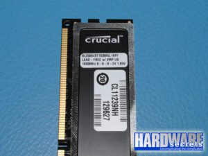
Figure 2: A DDR3-1600/PC3-12800 memory module with 8-8-8-24 timings
The operations that these numbers indicate are the following: CL-tRCD-tRP-tRAS-CMD. To understand them, bear in mind that the memory is internally organized as a matrix. This is where the data are stored at the intersection of the lines and columns.
- CL: CAS Latency. The time it takes between a command having been sent to the memory and when it begins to reply to it. It is the time it takes between the processor asking for some data from the memory and then returning it.
- tRCD: RAS to CAS Delay. The time it takes between the activation of the line (RAS) and the column (CAS) where the data are stored in the matrix.
- tRP: RAS Precharge. The time it takes between disabling the access to a line of data and the beginning of the access to another line of data.
- tRAS: Active to Precharge Delay. How long the memory has to wait until the next access to the memory can be initiated.
- CMD: Command Rate. The time it takes between the memory chip having been activated and when the first command may be sent to the memory. Sometimes this value is not announced. It usually is T1 (1 clock cycle) or T2 (2 clock cycles).
Usually, you have two options. The first one is to configure your PC to use the memory standard RAM timings, usually by setting memory configuration to “Auto” on the motherboard setup. The second one is to manually configure your PC to use lower memory timings.
Motherboard Timings
Notice that not all motherboards allow you to change the memory timings. Also, some motherboards may not be able to run at very low timings, and they may configure your memory module to run at a higher timing setting because of this.
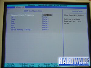
Figure 3: Configuration of memory timings at the motherboard setup
How does overclocking work?
When overclocking your memory, you may need to increase the memory timings in order to make the system run in a stable manner. Here is where something very interesting happens. Due to the increased timings, the memory may achieve a lower performance, even though it is now configured to run at a higher clock rate, due to the latency that was introduced.
That is another advantage of memory modules sold specifically for overclocking. The manufacturer, besides guaranteeing that your memory module will achieve the labeled clock rate, also guarantees that you will be able to keep the labeled timings up to the labeled clock.
To understand things easier.
For example, even though you may achieve 1,600 MHz (800 MHz x2) with DDR3-1333/PC3-10600 modules, on these modules it may be necessary to increase the memory timings, while on DDR3-1600/PC3-12800 ones the manufacturer guarantees that you will be able to achieve 1,600 MHz keeping the labeled timings.
Now we are going a step further as we will explain in detail each one of the memory timing parameters.
CAS Latency (CL) Impact on RAM Speed
As previously mentioned, CAS Latency (CL) is the best known memory parameter. It tells us how many clock cycles the memory will delay returning the requested data. A memory with CL = 7 will delay seven clock cycles to deliver data, while a memory with CL = 9 will delay nine clock cycles to perform the same operation. Thus, for two memory modules running at the same clock rate, the one with the lowest CL will be faster.
A direct example
Notice that the clock rate here is the real clock rate under which the memory module is running – i.e., half the rated clock rate. As DDR, DDR2, and DDR3 RAM memories can deliver two data per clock cycle, they are rated with double their real clock rate.
In Figure 4, you can see how CL works. We gave two examples, a memory module with CL = 7 and a memory module with CL = 9. The command in blue would be a “read” command.
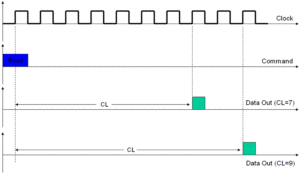
Figure 4: CAS Latency (CL)
A memory with CL = 7 will provide a 22.2% improvement on memory latency over a memory with CL = 9, considering that both are running at the same clock rate.
You can even calculate the time the memory delays until it starts delivering data. The period of each clock cycle can be easily calculated through the formula:
T = 1 / f
Thus, the period of each clock cycle of a DDR3-1333 RAM memory running at 1333 MHz (666.66 MHz clock) would be 1.5 ns (ns = nanosecond; 1 ns = 0.000000001 s). Keep in mind that you need to use the real clock rate, which is half of the labeled clock rate. So, this DDR3-1333 memory would delay 10.5 ns to start delivering data if it had CL =7, or 13.5 ns if it had CL = 9, for example.
Burst Mode explained
SDRAM, DDR, DDR2, and DDR3 RAM memories implement burst mode, where data stored in the next addresses can exit the memory at only one clock cycle. So, while the first data would delay CL clock cycles to exit the memory, the next data would be delivered right after. The prior data that has just come out from the memory, doesn’t have to wait for another CL cycle. Also, DDR, DDR2, and DDR3 memories deliver two data per clock cycle, and that is why they are labeled as having twice their real clock rate.
RAS to CAS Delay (tRCD) Impact on RAM Speed
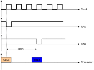
Figure 5: RAS to CAS Delay (tRCD)
Each memory chip is organized internally as a matrix. At the intersection of each row and column, we have a small capacitor that is in charge of storing a “0” or a “1” – the data. Inside the memory, the process of accessing the stored data is accomplished by first activating the row and then the column where it is located.
RAS and CAS
This activation is done by two control signals called RAS (Row Address Strobe) and CAS (Column Address Strobe). The less time there is between these two signals the better, as the data will be read sooner. RAS to CAS Delay or tRCD measures this time. In Figure 5 we illustrate this, showing a memory with tRCD = 3.
As you can see, RAS to CAS Delay is also the number of clock cycles taken between the “Active” command and a “read” or “write” command.
As with CAS Latency, RAS to CAS Delay works with the memory real clock (which is half of the labeled clock). The lower this parameter, the faster the memory will be, as it will start reading or writing data earlier.
RAS Precharged (tRP) Impact on RAM Speed
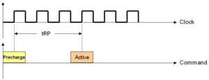
Figure 6: RAS Precharged (tRP)
After data is gathered from the memory, a command called Precharge needs to be issued, closi
ng the memory row that was being used and allowing a new row to be activated. RAS Precharge time (tRP) is the time taken between when the Precharge command and the next Active command can be issued. As we learned from the previous page, the Active command starts a read or write cycle.
In Figure 6, we are giving an example of a memory with tRP = 3.
As with the other parameters, RAS Precharge works with the memory real clock (which is half of the labeled clock). The lower this parameter, the faster the memory will be, as it will issue the Active command earlier.
Adding everything we’ve seen, the time elapsed between issuing the Precharge command and actually getting the data will be tRP + tRCD + CL.
Other Parameters Impacting RAM Timings
Let’s take a better look at the other two parameters, Active to Precharge Delay (tRAS) and Command Rate (CMD). As with the other parameters, these two parameters work with the memory real clock (which is half of the memory labeled clock). The lower these parameters, the faster the memory will be.
- Active to Precharge Delay (tRAS): After an Active command is issued, another Precharge command cannot be issued until tRAS has elapsed. So, this parameter limits when the memory can start reading (or writing) a different row.
- Command Rate (CMD): It is the time taken by the memory chip from being activated (through its CS – Chip Select – pin) and when any command can be issued to the memory. This parameter carries the letter “T” with it. Possible values are 1T or 2T, meaning one clock cycle or two clock cycles, respectively.
Frequently Asked Questions
How fast should RAM be for a gaming PC?
For gaming, we recommend RAM modules that are as fast as possible, for obvious reasons. For starters, video games these days not only take up quite a lot of the RAM but also separate that data. This is why you’ll need your RAM to access everything as quickly as possible for a seamless experience. You should go for dual-channel DDR4 or DDR5 RAM with a frequency of 3,000 MHz or more. Those modules can get quite expensive, but it’s way better than experiencing bottlenecks during intense gameplay sequences.
Do timings matter on RAM?
Overall, we certainly found that if you dig deep enough, you’ll discover that timings definitely matter. It won’t impact every game or application. However, it does make sense to at least consider timings when buying RAM, especially if you can get better timings. With that said, we only recommend buying RAM from trusted brands and from trusted retailers.
2 Reasons why your warranty can be voided.
Even if a RAM module’s warranty lasts a lifetime in theory, in practice that warranty can be easily voided. This could happen from two factors. First, if someone has tampered with the module in the past the warranty will be voided. Second, if there’s too much goo or liquid present on it the same thing will happen.
Is RAM speed limited by CPU?
Actually, it is the combination of CPU and motherboard which limits DIMM speed. DIMM speed will only go as high as the lower of the speed limits between the CPU and motherboard. For example, a CPU may support speed up to 1600 while a motherboard supports speeds up to 2400. However, DIMMs will go up to 1600. In short, your computer is only as fast as its weakest component.