Volta potential phase plate for in-focus phase contrast transmission electron microscopy (original) (raw)
Significance
Biological electron cryomicroscopy is limited by the radiation sensitivity of the samples and the consequent need to minimize exposure to the beam. This, in turn, results in low-contrast images with a poor signal-to-noise ratio. The current practice to improve phase contrast by defocusing results in contrast transfer functions necessitating image restoration to provide interpretable data. Phase plates enable in-focus phase contrast, but the existing ones, including the thin film Zernike-type phase plate, suffer from severe limitations, such as a short usable life span, fringing artifacts, and problems in using them in automated data acquisition procedures. The Volta phase plate presented here solves those problems and has the potential to become a practical solution for in-focus phase contrast in transmission electron microscopy.
Keywords: TEM, phase plate, Volta potential, phase contrast, cryo-EM
Abstract
We describe a phase plate for transmission electron microscopy taking advantage of a hitherto-unknown phenomenon, namely a beam-induced Volta potential on the surface of a continuous thin film. The Volta potential is negative, indicating that it is not caused by beam-induced electrostatic charging. The film must be heated to ∼200 °C to prevent contamination and enable the Volta potential effect. The phase shift is created “on the fly” by the central diffraction beam eliminating the need for precise phase plate alignment. Images acquired with the Volta phase plate (VPP) show higher contrast and unlike Zernike phase plate images no fringing artifacts. Following installation into the microscope, the VPP has an initial settling time of about a week after which the phase shift behavior becomes stable. The VPP has a long service life and has been used for more than 6 mo without noticeable degradation in performance. The mechanism underlying the VPP is the same as the one responsible for the degradation over time of the performance of thin-film Zernike phase plates, but in the VPP it is used in a constructive way. The exact physics and/or chemistry behind the process causing the Volta potential are not fully understood, but experimental evidence suggests that radiation-induced surface modification combined with a chemical equilibrium between the surface and residual gases in the vacuum play an important role.
Recent years have shown a steadily growing interest in in-focus phase contrast devices for transmission electron microscopy (TEM). Such devices are commonly referred to as “phase plates.” The “second wave” of phase plate research started more than 10 y ago and was motivated mainly by the challenges of biological TEM (1). There are several types of phase plates depending on the design and the physical phenomenon being used: thin film (2), electrostatic (3, 4), magnetic (5), laser (6), “tulip” (7), etc. However, for practical reasons most of these device types are not yet usable for applications (8, 9). The only phase plate that has demonstrated advantages in real-world cryo-EM applications is the thin-film Zernike phase plate (ZPP) (10, 11).
The thin-film ZPP consists of a thin (∼20 nm) material film, typically amorphous carbon, with a small (∼1 μm) hole in the center (12). The film thickness is selected such that it causes ∼π/2 phase shift for electrons passing through the film (1). The phase plate is positioned at the back focal plane of the objective lens so that the central beam of unscattered electrons passes through the hole. There have been successful ZPP applications in single-particle analysis (11, 13), cryo-tomography (10, 13, 14), and single-image cryo-EM (15, 16). However, the ZPP has a few limitations that affect its overall performance and ease of use. The main unsolved issue is the short life span of the phase plate (12). Following installation into the TEM, its performance gradually deteriorates independent of its use. This behavior is commonly referred to as “aging” of the phase plate. The typical usable lifetime of a carbon film ZPP is about a week, after which it must be exchanged. Another problem is the hole of the phase plate. Its size is a subject of a compromise—a smaller hole provides better contrast for large-specimen features but is more difficult to align and maintain centered on the beam and vice versa. The sharp onset of the contrast transfer function (CTF) at the phase plate hole edge produces fringes around high-contrast features in the image (15, 17). The fringing can be demodulated by software postprocessing, but the results are not perfect (17, 18). Another open issue is the current lack of software and hardware support for automated data acquisition with the ZPP.
An ideal phase plate would have a central phase-shifting area with exactly the same size and position as the central diffraction beam. One possibility to realize that in practice is to use the beam itself for the creation of the phase-shifting area. In fact, beam-generated phase plates have been proposed and tested (19–21). Early attempts used beam-induced contamination and/or electrostatic charging on the surface of a material as the central phase-shifting zone. The results show a significant contrast increase for organic and inorganic samples. However, apart from the improved contrast, all previous reports share a common problem—CTF distortion due to electrostatic charging characterized by rapid oscillations near the Fourier space center (21, 22). Such a CTF does not correspond to the theoretical phase-CTF model and cannot be easily fitted or corrected.
Here, we present a new type of beam-created phase plate that we call the Volta phase plate (VPP). The name was chosen in accordance with our hypothesis that a beam-induced Volta potential resulting from changes in the properties of the film is the main source of the phase shift. Unlike previously reported beam-created phase plates, the VPP does not suffer from CTF deformations and it does not change its properties over time.
Results and Discussion
Heated Amorphous Carbon Films Show an Unusual Beam-Induced Phase Shift Behavior.
To test the performance of various materials for the preparation of ZPPs, we developed the beam-induced phase shift (BIPS) method (Materials and Methods). It measures the phase shift experienced by the central diffraction beam when a continuous film of the material is placed at the back-focal plane of the objective lens. The resulting phase shift vs. dose curve is a quantitative measure of the stability of the film to electron beam irradiation. During testing of heated amorphous carbon films with the BIPS method, we noticed a rather peculiar behavior. Fig. 1_A_ shows BIPS curves for a 12-nm amorphous carbon film. Movie S1 shows the typical evolution of the CTF during a BIPS series. Both the curves in Fig. 1_A_ and Movie S1 indicate that, after the film has been in the microscope for more than a few days, the central beam experiences a phase advance relative to the scattered beams. This result is opposite in sign to what would be expected if beam-induced electrostatic charging would cause it. Beam irradiation produces positive charges on nonconducting surfaces (21, 22), which leads to phase retardation (22). The phase advance observed here means that the irradiated area has a negative potential, which cannot be a result of beam-induced electrostatic charging. Fig. S1 illustrates the different potentials associated with a conducting material in vacuum. The Volta potential is the potential immediately above the surface of the material and is equal to the difference between the inner and the surface potentials. A negative Volta potential can explain the observed phase shift. Fig. S2_A_ shows the result from a numerical simulation of the 3D potential distribution above a grounded conductor with a constant potential patch on the surface. Fig. S2_B_ contains a plot of the integrated along z potential profile. An electron traveling along z will experience a phase shift proportional to the integrated potential (22). Our hypothesis is that the strong irradiation by the central diffraction beam causes local changes in the properties of the carbon film that lead to changes in the inner and/or surface potentials. Such changes will lead to a local modification of the Volta potential, which in turn will cause a phase shift. A variation of the inner potential will also cause a phase shift difference within the film, but because the film thickness is very small compared with the 3D potential distribution above and below the film, the effect will be negligible compared with that of the Volta potential (the phase shift is proportional to the path integrated potential). The curve in Fig. S2_B_ shows that the phase shift is highly localized and thus will not influence and cause deformation to the CTF outside the central potential patch. The size of the 3D distribution scales linearly with the size of the patch, so the phase shift will also be linearly proportional to the patch size, e.g., keeping the potential constant a twofold bigger patch will produce twice the phase shift. It must be noted that, unlike the beam-induced charging models (21, 22), in the Volta potential model the net charge of the film is zero and the potential change is a result of changes in the surface and/or inner potentials.
Fig. 1.

Beam-induced phase shift (BIPS) as a function of the total dose for a 12-nm–thick amorphous carbon film. The phase shift plotted is that of the central beam relative to the scattered beams and a positive value means phase advance. Experimental data are shown with symbols; the solid lines represent double asymptotic exponential fits. (A) BIPS curves for a film heated to 225 °C, beam current of 1 nA. The legend shows the film age, measured from the moment it was inserted into the microscope, and the beam diameter on the film (25 nm, on-plane; 1,000 nm, off-plane). (B) BIPS curves on-plane (25-nm beam diameter) at different temperatures; film age was 51 d, and beam current was 1 nA. The film was kept for ∼24 h at 150 °C before the first measurement and then for ∼1 h at the other two temperatures before their respective measurements. (C) BIPS curves on-plane (25-nm beam diameter) with different beam currents; film age was 52 d, and temperature was 225 °C.
The BIPS Is Responsible for the Aging of ZPPs.
The evolution of the “on-plane” (25-nm beam) BIPS curves in Fig. 1_A_ with time clearly illustrates the aging behavior of amorphous carbon. On day 1 after installation into the microscope (black squares), there was very little negative phase shift. After a week (blue circles), the phase shift had changed its sign and increased. The subsequent tests show that, with time, the BIPS behavior stabilizes. This closely matches and can explain the aging behavior of ZPPs, whereas in the first few days the phase shift is solely caused by the inner potential within the film after which an additional parasitic phase shift develops around the central hole probably due to Volta potential effects.
Effect of Temperature on the BIPS.
Fig. 1_B_ shows BIPS measurements at different temperatures. The curves indicate that increasing the film temperature reduces the BIPS. These results suggest that temperature can in principle be used to control the phase shift albeit within a limited range.
The BIPS Is a Function of the Total Dose and Not of the Dose Rate.
BIPS data for different beam currents are plotted in Fig. 1_C_. The beam current was varied by changing the spot size setting of the microscope. Apart from small deviations, the curves indicate that the BIPS is a function of the total dose and does not depend noticeably on the dose rate. It must be noted that, at the lower beam currents (0.5 and 0.25 nA), the beam diameter on the film was smaller than the beam diameter of the 1-nA beam, but this did not produce a significant change in the behavior of the BIPS.
The Buildup of BIPS Contains at Least Two Components.
Good fits (solid lines) of the BIPS data in Fig. 1 A and B could be obtained with a function comprising the sum of two asymptotic exponents suggesting that there are at least two processes involved (Double Asymptotic Exponent Fits of the BIPS Data). The first process has a small characteristic dose of a few nanocoulombs and is responsible for the steep rise of the phase shift in the beginning. The second process governs the slow gradual increase of the phase shift after the first process. The results of the fits are presented in Tables S1 and S2.
Relaxation Behavior of Phase Shift Patches on Heated Amorphous Carbon Films.
The phase shift patches created by the beam can be observed in a low-magnification mode if sufficient defocus is applied (a few millimeters underfocus). Fig. 2 shows low-magnification images of 1-μm–diameter beam spots on the carbon film. Beam-created spots have been reported in the past and are known as the “Berriman effect” (23). The Berriman effect is related to beam-induced charging and the spots appear darker than the background. The spots in Fig. 2 are brighter than the background, which is another confirmation that the BIPS has an opposite sign to and is not due to beam-induced charging. Fig. 2 A and B contains images of a beam spot (white arrow) with 15-mm underfocus and in-focus, respectively. The spot is not visible in the in-focus image (Fig. 2_B_), which confirms that the effect is purely due to phase shift and not due to beam-induced etching of the film. Fig. 2 C and D shows a beam spot (black arrow) in the vicinity of a focused ion beam (FIB)-milled hole in the film (white arrow). The first image (Fig. 2_C_) was taken immediately after creating the beam spot. The second one (Fig. 2_D_) was taken 5 d later. The beam spot had disappeared after 5 d, suggesting that the film properties recover after a period. Furthermore, Fig. 2_E_ shows an image of a freshly created beam spot (white arrow) next to beam spots created more than 10 d earlier (black arrows). The old beam spots have not just recovered but also show a slight overshoot in a sense that they are slightly darker than the surroundings. This suggests that, in the long term, the changes induced by electron irradiation result in a slightly different state of the film with a phase shift marginally higher than the original one. The contrast of the darker spots is less than 1/10 of the contrast of the freshly created spot, which means that the overshoot in terms of phase shift is ∼π/20 (assuming the original spot was π/2). Such a phase shift will not produce a noticeable CTF distortion if an old spot happens to be in the vicinity of the central beam.
Fig. 2.

Low-magnification images of 1-μm beam spots on 12-nm–thick amorphous carbon film kept at 225 °C. The spots were created with a beam current of 1 nA and a dose of 100 nC (100 s of irradiation). (A and B) The same spot observed with (A) 15-mm underfocus and (B) in-focus. (C and D) A beam spot (black arrow) next to a FIB-produced hole in the film (white arrow). The first image (C) was taken immediately after the spot was created. The second image (D) was taken 5 d later. (E) A freshly created beam spot (white arrow) next to beam spots created more than 10 d earlier (black arrows). Defocus for C–E: 50-mm underfocus. (Scale bars: 5 μm.)
The Recovery Speed of Phase Shift Patches Is Temperature Independent but Is Influenced by Residual Gas Concentration.
The long-term behavior of beam-created spots is shown in Fig. 3. The results are quite surprising in that the recovery time of the phase shift patches does not seem to depend on the temperature of the film. One would expect that a higher temperature will speed up the recovery process but that is not the case. Unlike temperature, the use or not use of the liquid nitrogen-cooled anticontamination device (ACD) of the microscope had a significant impact on the recovery speed. Using the ACD slowed down the process ∼1.4 times. This suggests that residual gases in the vacuum, such as water, vacuum oils, etc., play an important role in the recovery process. This also provides an indirect indication that the BIPS is probably due to changes in surface chemistry rather than changes inside the bulk film. The solid curves in Fig. 3 are double-exponential decay fits of the 225 °C data. With the ACD OFF, the two time constants are 47 and 1,180 min. With the ACD ON, both constants increase ∼1.4 times to 65 and 1,650 min. It is not clear whether the two recovery time constants are related to the two components of the phase shift buildup.
Fig. 3.

Long-term behavior of beam-created spots on amorphous carbon film. The average intensity of a 0.5-μm beam spot was measured relative to the background and then normalized by the original spot intensity. All spots were created at 225 °C after which the temperature was set to the indicated in the legend temperature for each measurement. The legend also indicates whether the anticontamination device (ACD) was used (ON) or not (OFF) during the relaxation period.
A Surface Chemistry Hypothesis About the Volta Potential and the BIPS.
The most interesting question concerning the BIPS is about the mechanism underlying it. The experimental facts suggest that it is not beam-induced electrostatic charging. An obvious explanation would be beam-induced etching of the film, but the images in Fig. 2 A and B disprove that. The strong dependence of the beam spot recovery time on the use or not of the ACD (Fig. 3) indicates that most probably the phenomenon is related to the surface chemistry of the film. Our hypothesis is that beam irradiation causes local desorption of the chemisorbed species, which leads to a local change in the work function and thus the Volta potential. The negative sign of the observed Volta potential indicates that the work function in the irradiated area is lower than in the surroundings. Oxidation of graphene (24) and carbon nanotubes (25) can significantly increase (up to 60%) their work functions, and thus an oxidized equilibrium state outside the central beam area in combination with a local beam-induced reduction are a good candidate for explaining the observed lowering of the work function at the beam spot. The lack of dependence of the recovery speed on the temperature of the phase plate is rather puzzling and cannot be explained by a simple adsorption model. In general, the adsorption rate is proportional to the bombardment rate of gas molecules on the surface and to the sticking probability. The bombardment rate is a function of the gas temperature and pressure and is thus affected mainly by the ACD. On the other hand, the sticking probability should be affected by the temperature of the film, but the experimental data show no such effect. Based on the limited data, we can only conclude that in microscopes with good vacuum and/or with large cryoshields beam-created spots will take longer to recover.
The “development” of the BIPS with time (Fig. 1_A_) and the aging of the ZPP in the first week after installation suggest that the initial state of the film surface is different from the equilibrium state. It takes about a week for the carbon film to transition from its initial state after preparation to its equilibrium state inside the microscope possibly due to a change in the chemical composition of the surface.
The dynamics of BIPS buildup indicate that there are at least two characteristic processes involved—one fast and one slow (Double Asymptotic Exponent Fits of the BIPS Data). This can be explained by another hypothesis—the fast process is the surface transition at the central beam spot where the current density is very high followed by a second process of gradual enlargement of the surface potential patch. The enlargement could be due to low-angle scattered electrons from the specimen and/or secondary/auger electrons emitted from the central beam spot on the phase plate reacting and modifying the surface around the central spot.
Without additional experimental evidence from other analytical methods, we can only speculate about the exact physics or chemistry behind the observed behavior of the carbon film. Techniques such as tip-enhanced Raman spectroscopy, Kelvin probe force microscopy, high-resolution electron energy loss spectroscopy, or X-ray photoelectron spectroscopy may be able to provide the necessary information. However, observations will be quite challenging because the specimen is in the form of a very thin free-standing film that must be kept heated in a vacuum for several days before it reaches the equilibrium state showing the Volta potential effect.
The BIPS of Heated Amorphous Carbon Films Is Suitable for a Phase Plate.
As shown by the curves in Fig. 1, the phase shift has the proper sign, with the central beam experiencing phase advance, and the proper magnitude of approximately π/2. This makes it suitable for a phase plate—the VPP. Before its use, a phase-shifting spot must be created by preirradiation with the central diffraction beam for a period. The necessary time to reach a desired phase shift with a given beam current can be calculated from the data in Fig. 1_C_.
CTF Performance of the VPP.
The fast Fourier transforms (FFTs) of high-magnification images of a thin amorphous carbon film specimen taken without and with a VPP are shown side by side in Fig. 4_A_. The CTFs show a very good complementary match with a phase shift close to π/2 and no distortions in the phase plate CTF. Fig. 4_B_ shows rotationally averaged and background normalized profiles of the FFTs in Fig. 4_A_. CTF fits of both profiles are shown with thin black lines and are difficult to see because for the most part they overlap with the experimental data, indicating a good fit. The CTF model for the VPP image included phase shift as an additional parameter. The fitted defocus values were 487 nm without VPP and 482 nm with VPP, both underfocus. The practically negligible defocus difference of 5 nm confirms that the VPP does not suffer from beam-induced charging and its consequent CTF deformation. The fit of the VPP CTF gave a phase shift value of 0.54π, which is very close to the ideal π/2. The curves and the fits also indicated that the signal with a VPP is ∼18% less than the signal without a phase plate. This value is higher than what would be expected based on scattering by the phase plate film. The total mean free path of amorphous carbon for 200-kV electrons is ∼92 nm (17). A 12-nm–thick film will thus scatter ∼12% of the incident electrons. Without a specimen, we measured a 7% drop in beam intensity when the phase plate was inserted. This drop is mainly due to elastic scattering by the phase plate because of the higher scattering angles for elastic events. The higher than expected signal loss of ∼18% is probably a combination of several factors. The first one is the increase of the noise background due to inelastic scattering by the phase plate. A second noise source is the “phase noise” due to roughness of the phase plate film, but this is a minor effect: 10% roughness of a 12-nm–thick film is 1.2 nm valley to peak and will result in ∼0.02π phase modulation, which is practically negligible. A third factor with the VPP is the fact that the central beam passes through the film rather than through a hole as is the case for ZPPs. Thermal noise or oscillations of the Volta potential at the position of the central beam could be contributing to the noise in the image, but without additional experimental evidence it is difficult to speculate about such factors.
Fig. 4.

(A) Side-by-side FFTs of high-magnification images taken without and with a VPP. The CTFs demonstrate a very good complementary match with no deformation. (B) Rotationally averaged and background normalized profiles of the FFTs in A. Both profiles fit very well the theoretical CTF model (black lines), which confirms the absence of electrostatic charging distortion. The VPP CTF (red line) indicates about 18% signal loss compared with that without a phase plate (blue line). Defocus: 500 nm. (Scale bar: 1 nm−1.)
The VPP Works Best On-Plane.
Fig. S3 shows the low-frequency portions of rotationally averaged FFTs of images taken with the VPP on-plane and off-plane with the same central beam sizes (25 and 1,000 nm) as the BIPS curves in Fig. 1_A_. The solid arrows indicate the expected cut-on periodicities based on the beam size (from equation 3 in ref. 1). The dashed arrows point at the approximate positions of the observed cut-on periodicities. The phase shift patch of the smaller beam (dashed red arrow) is ∼11 times larger (∼285-nm patch diameter) than the beam itself (25 nm; solid red arrow), and from the simulations in Fig. S2 it must have a Volta potential of approximately −1.1 V to produce π/2 phase shift. The enlargement of the patch could be due to low-angle scattered electrons and/or secondary/auger electrons activating the area around the central beam as already discussed in the hypothesis part. The effective patch size of the large beam (dashed blue arrow) is ∼0.6 times the size of the beam (solid blue arrow), which can be explained by the fact that the phase plate is off-plane, which causes blurring of the phase shift profile in Fourier space. The curves in Fig. S3 show that using the VPP on-plane provides better performance in terms of lower cut-on periodicity (dashed arrows), which will result in better contrast for large-specimen features. The curves also illustrate the soft cut-on of the VPP with the CTF raising smoothly toward the first maximum, which prevents fringing artifacts from appearing in the image. Another advantage of using the VPP on-plane is the proper phase shift of ∼π/2. When used off-plane (Fig. 1_A_, hollow green triangles), the VPP produces too much phase shift, which is undesirable because it produces reduced or even inverted contrast (17).
Heating of the Carbon Film Is Essential for the Proper Operation of the VPP.
Fig. S4 shows side-by-side FFTs from BIPS series acquired with the film at 60 °C. Movie S2 contains the complete series. Early in the series, a zero appears close to the center of the FFT and moves outward as the series progress. This is a typical behavior for beam-induced contamination and charging. The CTF maxima move outward, indicating that the central beam experiences phase retardation relative to the scattered beams. The retardation is caused by the increase in thickness and/or positive charging at the position of the beam. Images taken in such a regime may show overall increase in contrast, but the CTF is deformed and cannot be fitted or corrected using the standard phase-CTF model. Previous attempts with beam-created phase plates (19–21) did not use heating, which led to a poor CTF performance.
The VPP Performs Better than a ZPP.
A comparison between a ZPP and a VPP images of lacey carbon film is presented in Fig. 5. The ZPP image (Fig. 5_A_) has lower overall contrast than the VPP image (Fig. 5_C_) and shows fringing artifacts, especially around the film edges. The image in Fig. 5_B_ is a fringe reduction software-filtered (18) version of the image in Fig. 5_A_. The overall contrast and the fringing over the film were improved, but the fringing inside the holes remains visible. Even after software filtration the ZPP image (Fig. 5_B_) cannot match the contrast and the fidelity of the VPP image (Fig. 5_C_).
Fig. 5.
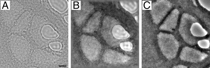
Images of lacey carbon film acquired with (A) a ZPP and (C) a VPP. The image in B is a fringe reduction software-filtered version of the ZPP image in A. (Scale bar: 20 nm.)
The VPP Is Suitable for Cryo-EM Observations.
Cryo-EM images of the tip of a vitrified worm sperm flagellum (Lumbricus terrestris) are shown in Fig. 6. The conventional image (Fig. 6_A_) was acquired with a relatively high defocus of 5 μm but still has lower overall contrast than the VPP image (Fig. 6_B_). The microtubules inside the flagellum are well visualized in both images (solid black arrows). However, low-density proteins on the outside and on the inside of the cell membrane (dashed black arrows) are easier to see and locate in the VPP image. The VPP image also does not exhibit defocus artifacts, such as the Fresnel fringes around the gold nanoparticles and a contaminant particle (white arrows).
Fig. 6.

Cryo-EM images of vitrified worm sperm flagellum (A) without and (B) with a VPP. The black solid arrows indicate microtubules inside the flagellum. The black dashed arrows point to proteins on the outside and the inside of the membrane. The white arrows point at a gold fiducial marker and a contaminant. Defocus: (A) 5-μm underfocus, (B) close to focus. (Scale bar: 100 nm.)
Conclusions
Heated amorphous carbon films display a peculiar behavior of a negative Volta potential at the place of electron beam irradiation. This behavior is responsible for the reduced performance with age of thin film ZPPs. The newly proposed VPP uses this behavior constructively to generate a phase shift with the same sign and similar magnitude to that of a ZPP. The phase shift is created at the position of the central diffraction beam and develops with the accumulated dose. Before use, the VPP must be preconditioned by continuous irradiation on a fresh area of the film for about a minute to generate the phase shift. The VPP solves two major issues of the ZPP—the aging and the fringing. Images taken with the VPP do not show fringing artifacts but just a smooth bright halo around high-contrast edges due to the smooth onset of the phase shift. The best operation mode for the VPP is “on-plane” with the central diffraction beam crossover on the phase plate plane. In this mode, the phase shift is close to π/2 and the phase plate has the lowest possible cut-on frequency. Because the phase shift is created at the position of the beam, the VPP does not require precise alignment, which means that automation of the VPP will be much easier than other types of phase plates. Heating of the carbon film is crucial for the proper operation of the VPP. Without or with insufficient (<100 °C) heating, beam-induced contamination and charging become the dominant effect, resulting in a phase shift with opposite sign to what is desired and CTF deformation. The CTF of the VPP shows an excellent agreement with the theoretical model confirming the absence of beam-induced electrostatic charging. The phase shift patches created on the VPP during use disappear after a few days, and the same areas of the phase plate can be reused. The VPP has a very long usable life and we expect that exchanges of the phase plate will only be necessary in case of an accidental physical damage to the film or dust/particulate contamination introduced when the microscope column is vented for servicing. There are still open questions that require further investigation. The exact physics and chemistry behind the negative Volta potential are unknown. Experimental evidence suggests that the effect is probably related to a chemical equilibrium between the surface of the carbon film and the residual gases in the vacuum. Another issue that must be studied further is the higher than expected signal loss with the VPP. Apart from that, the VPP promises to be a user friendly and maintenance-free solution for in-focus phase contrast imaging in TEM.
Materials and Methods
All experiments were performed on an FEI Tecnai F20 (FEI) 200-kV electron microscope equipped with an FEI Eagle 4K CCD camera. The objective aperture holder was replaced with a newly designed ceramic phase plate holder with built-in heater (Fig. S5). The holder can accommodate one heated phase plate and two nonheated objective lens apertures, all 3 mm in diameter. The phase plates were prepared by vacuum evaporation of carbon on a freshly cleaved mica surface by a BAL-TEC MED-020 (currently Leica Microsystems) electron beam evaporator. The films were transferred onto 3-mm titanium TEM grids, Agar G2462TI (Agar Scientific), by floating off on a water surface followed by lowering of the water level to gently deposit the films onto the preimmersed grids. The thickness of the film on the prepared grids was measured to be 12 ± 1 nm by TEM observation of the film profile at a folded edge (12).
The BIPS series method for characterization of the performance of thin films as phase plate candidates was as follows. The film under investigation was positioned at the back focal plane of the objective lens and heated to ∼200 °C. The spot size, the condenser aperture, and the field emission gun extraction voltage were selected to provide 1-nA beam current. The second condenser lens was adjusted for either on-plane condition (central diffraction beam crossover on the phase plate plane) or with an offset value from the on-plane condition so that the central beam spot at the back-focal plane was 1 μm in diameter (off-plane condition). The offset value (approximately −0.2% with a 50-μm condenser aperture) was initially determined by comparing the beam spot to a 1-μm FIB-prepared hole in the film. An amorphous carbon film was used as a specimen and the objective lens defocus was adjusted for the FFT of the image to show ∼10 CTF maxima (∼15-μm underfocus). The microscope magnification was 29,000×, resulting in a pixel size of 0.75 nm with one time binning on the camera. Image series were then collected from a fresh (nonirradiated) area of the film under investigation positioned at the back focal plane. The series consisted of 50 images with 2-s exposure each, which resulted in a total dose for the series of 100 nC. The rotationally averaged FFT of each image in the series was fitted with an extended CTF model, which included phase shift in addition to defocus and spherical aberration. The final result is in the form of a phase shift vs. accumulated dose curve.
Supplementary Material
Supplementary File
Supplementary File
Supplementary File
Acknowledgments
We thank Günther Gerisch and Maria Ecke for providing the worm sperm sample. We are grateful to FEI for providing material and financial support for this project.
Footnotes
Conflict of interest statement: B.B. is a full-time employee of FEI.
References
- 1.Danev R, Nagayama K. Transmission electron microscopy with Zernike phase plate. Ultramicroscopy. 2001;88(4):243–252. doi: 10.1016/s0304-3991(01)00088-2. [DOI] [PubMed] [Google Scholar]
- 2.Nagayama K, Danev R. Phase contrast electron microscopy: Development of thin-film phase plates and biological applications. Philos Trans R Soc Lond B Biol Sci. 2008;363(1500):2153–2162. doi: 10.1098/rstb.2008.2268. [DOI] [PMC free article] [PubMed] [Google Scholar]
- 3.Walter A, et al. Practical aspects of Boersch phase contrast electron microscopy of biological specimens. Ultramicroscopy. 2012;116:62–72. doi: 10.1016/j.ultramic.2012.03.009. [DOI] [PubMed] [Google Scholar]
- 4.Frindt N, et al. In-focus electrostatic Zach phase plate imaging for transmission electron microscopy with tunable phase contrast of frozen hydrated biological samples. Microsc Microanal Canada. 2014;20(1):175–183. doi: 10.1017/S1431927613013901. [DOI] [PubMed] [Google Scholar]
- 5.Edgcombe CJ, et al. Characterisation of ferromagnetic rings for Zernike phase plates using the Aharonov-Bohm effect. Ultramicroscopy. 2012;120:78–85. doi: 10.1016/j.ultramic.2012.06.011. [DOI] [PubMed] [Google Scholar]
- 6.Müller H, et al. Design of an electron microscope phase plate using a focused continuous-wave laser. New J Phys. 2010;12:12. doi: 10.1088/1367-2630/12/7/073011. [DOI] [PMC free article] [PubMed] [Google Scholar]
- 7.Buijsse B, et al. Design of a hybrid double-sideband/single-sideband (schlieren) objective aperture suitable for electron microscopy. Ultramicroscopy. 2011;111(12):1688–1695. doi: 10.1016/j.ultramic.2011.09.015. [DOI] [PMC free article] [PubMed] [Google Scholar]
- 8.Danev R, Nagayama K. Phase plates for transmission electron microscopy. Methods Enzymol. 2010;481:343–369. doi: 10.1016/S0076-6879(10)81014-6. [DOI] [PubMed] [Google Scholar]
- 9.Glaeser RM. Invited review article: Methods for imaging weak-phase objects in electron microscopy. Rev Sci Instrum. 2013;84(11):111101. doi: 10.1063/1.4830355. [DOI] [PMC free article] [PubMed] [Google Scholar]
- 10.Dai W, et al. Visualizing virus assembly intermediates inside marine cyanobacteria. Nature. 2013;502(7473):707–710. doi: 10.1038/nature12604. [DOI] [PMC free article] [PubMed] [Google Scholar]
- 11.Rochat RH, et al. Seeing the portal in herpes simplex virus type 1 B capsids. J Virol. 2011;85(4):1871–1874. doi: 10.1128/JVI.01663-10. [DOI] [PMC free article] [PubMed] [Google Scholar]
- 12.Danev R, Glaeser RM, Nagayama K. Practical factors affecting the performance of a thin-film phase plate for transmission electron microscopy. Ultramicroscopy. 2009;109(4):312–325. doi: 10.1016/j.ultramic.2008.12.006. [DOI] [PMC free article] [PubMed] [Google Scholar]
- 13.Murata K, et al. Zernike phase contrast cryo-electron microscopy and tomography for structure determination at nanometer and subnanometer resolutions. Structure. 2010;18(8):903–912. doi: 10.1016/j.str.2010.06.006. [DOI] [PMC free article] [PubMed] [Google Scholar]
- 14.Fukuda Y, Nagayama K. Zernike phase contrast cryo-electron tomography of whole mounted frozen cells. J Struct Biol. 2012;177(2):484–489. doi: 10.1016/j.jsb.2011.11.018. [DOI] [PubMed] [Google Scholar]
- 15.Fukuda Y, Fukazawa Y, Danev R, Shigemoto R, Nagayama K. Tuning of the Zernike phase-plate for visualization of detailed ultrastructure in complex biological specimens. J Struct Biol. 2009;168(3):476–484. doi: 10.1016/j.jsb.2009.08.011. [DOI] [PubMed] [Google Scholar]
- 16.Yamaguchi M, Danev R, Nishiyama K, Sugawara K, Nagayama K. Zernike phase contrast electron microscopy of ice-embedded influenza A virus. J Struct Biol. 2008;162(2):271–276. doi: 10.1016/j.jsb.2008.01.009. [DOI] [PubMed] [Google Scholar]
- 17.Danev R, Nagayama K. Optimizing the phase shift and the cut-on periodicity of phase plates for TEM. Ultramicroscopy. 2011;111(8):1305–1315. doi: 10.1016/j.ultramic.2011.04.004. [DOI] [PubMed] [Google Scholar]
- 18.Danev R, Kanamaru S, Marko M, Nagayama K. Zernike phase contrast cryo-electron tomography. J Struct Biol. 2010;171(2):174–181. doi: 10.1016/j.jsb.2010.03.013. [DOI] [PubMed] [Google Scholar]
- 19.Johnson HM, Parsons DF. Enhanced contrast in electron microscopy of unstained biological material. 3. In-focus phase contrast of large objects. J Microsc. 1973;98(1):1–17. doi: 10.1111/j.1365-2818.1973.tb03799.x. [DOI] [PubMed] [Google Scholar]
- 20.Unwin PN. Phase contrast electron microscopy of biological materials. J Microsc. 1973;98(3):299–312. doi: 10.1111/j.1365-2818.1973.tb03834.x. [DOI] [PubMed] [Google Scholar]
- 21.Malac M, Beleggia M, Kawasaki M, Li P, Egerton RF. Convenient contrast enhancement by a hole-free phase plate. Ultramicroscopy. 2012;118:77–89. doi: 10.1016/j.ultramic.2012.02.004. [DOI] [PubMed] [Google Scholar]
- 22.Danov K, Danev R, Nagayama K. Electric charging of thin films measured using the contrast transfer function. Ultramicroscopy. 2001;87(1-2):45–54. doi: 10.1016/s0304-3991(00)00061-9. [DOI] [PubMed] [Google Scholar]
- 23.Downing KH, McCartney MR, Glaeser RM. Experimental characterization and mitigation of specimen charging on thin films with one conducting layer. Microsc Microanal. 2004;10(6):783–789. doi: 10.1017/s143192760404067x. [DOI] [PubMed] [Google Scholar]
- 24.Kumar PV, Bernardi M, Grossman JC. The impact of functionalization on the stability, work function, and photoluminescence of reduced graphene oxide. ACS Nano. 2013;7(2):1638–1645. doi: 10.1021/nn305507p. [DOI] [PubMed] [Google Scholar]
- 25.Ago H, et al. Work functions and surface functional groups of multiwall carbon nanotubes. J Phys Chem B. 1999;103(38):8116–8121. [Google Scholar]
Associated Data
This section collects any data citations, data availability statements, or supplementary materials included in this article.
Supplementary Materials
Supplementary File
Supplementary File
Supplementary File