PCB Board Manufacturer | Top PCB Fabrication Company (original) (raw)
WellPCB is a global embedded PCB manufacturer providing end-to-end PCB fabrication services with advanced DFM support, strict IPC-A-610 Class 3 quality standards. We provide quick-turn PCB prototyping and production.
- 72-hour lead time for standard 1 to 12-layer PCB prototypes
- PCB fabrication with copper weights up to 28 oz, HDI support, and up to 64-layer stackups
- ISO 9001, RoHS, and UL-certified PCB manufacturer
- Full turnkey PCB assembly services
4.8  google
TrustPilot
![]()
ISO9001 ISO13485
ISO14001

IATF
16949
![]()
IPC-A-610H International
Certification

Fully Automated
AOI Inspection
![]()
![]()
- Home
- PCB Manufacturer
Full-Cycle PCB Manufacturing
You Can Rely On
At WellPCB, we manage every stage of your PCB project under one roof, from DFM optimization and material selection to fabrication, assembly, testing, and global delivery.
By keeping all core processes in-house across our ISO-certified facilities, we maintain strict control over quality, lead time, and cost, ensuring your printed circuit boards meet the highest industry standards from prototype to production.
Technical Capabilities & Specifications:
Our advanced fabrication capabilities include complex rigid, flex, and rigid-flex printed circuit boards with capabilities from 1 to 64 layers. Our in-house fabrication lines handle precision specifications including 1.8 mil trace/space, 3 mil microvias, and PCB fabrication with copper weights up to 28 oz with HDI support and up to 64-layer stackups.
We offer comprehensive surface finishes including HASL, Lead free HASL, ENIG(+ G/F), Immersion silver/Tin, OSP, ENEPIG, and bare copper to meet diverse application requirements.
Our Capabilities As a PCB Manufacturer
We support PCB stackups from 1 to 64 layers, including complex high-density interconnect (HDI) architectures such as 1+n+1 through 8+n+8 and 18L any-layer interconnect structures.
Our via technologies include blind, buried, via-in-pad, stacked microvias, and via-in-via designs, supporting an aspect ratio of up to 40:1 for robust multilayer PCB performance in high-reliability environments.
| Feature | Specification |
|---|---|
| Supported Layer Count | 1 to 64 layers |
| HDI Stack-Up Architectures | Configurations such as 1+n+1, 2+n+2, up to 8+n+8; 18L any-layer interconnect supported. |
| Via Technologies | Blind vias, buried vias, stacked microvias (laser-formed, 4 to 6 mil), via-in-pad (VIP), via-in-via, skip vias. Supports staggered or stacked via structures with copper-filled and resin-filled options. Laser via diameter: 3 to 6 mil (0.075 to 0.15 mm); mechanical via minimum: 0.1 mm. |
| Maximum Aspect Ratio | Up to 40:1 for high-reliability multilayer builds. |
| Minimum Drill Size | Mechanical: 0.1 mm; Laser: 3 to 6 mil (0.076 to 0.15 mm). |
| Finished Board Thickness | 0.1 to 12 mm. |
| Via Copper Plating Thickness | ≥25 µm (1 mil); uniformity within ±10%. |
| Dielectric Thickness Control | Prepreg layers down to 0.075 mm ±10% precision. |
| Stack-Up Symmetry Options | Symmetrical and bookbinder (asymmetrical) stack-ups are supported. |
| Impedance Control Support | Supported on specified layers; single-ended and differential; tolerance ±5% |
Our fabrication capabilities achieve trace widths and spacings down to 1.8 mil (0.045 mm), ideal for fine-pitch components and HDI layouts. We support PTH diameters down to 0.08 mm, minimum routed slot widths of 0.5 mm, and silkscreen minimum line widths of 4 mil.
Solder mask dam resolution is 3 mil, with routing tolerance maintained within ±0.04 mm for precise board outlines and mechanical features.
We manufacture PCBs with finished copper weights ranging from 0.5 oz to 28 oz (≈1000 μm), supporting both signal integrity and high current applications.
Final board thickness options span from 0.1 mm to 12 mm, enabling fabrication of ultra-thin flex boards to thick, heavy-copper PCBs for power electronics.
WellPCB offers a broad spectrum of PCB base materials, including standard FR4, high-Tg FR4, halogen-free, and CEM-3 for general applications.
For specialized performance, we fabricate with Rogers RO4003 and RO4350 for RF circuits, ceramic substrates for thermal stability, polyimide for flexible PCBs, and metal-core materials such as aluminum and copper for LED and power conversion boards.
We support all mainstream and advanced surface finishes, including HASL (leaded and lead-free), ENIG (Electroless Nickel Immersion Gold), ENEPIG, OSP (Organic Solderability Preservative), immersion silver, and immersion tin.
Selective finish combinations such as ENIG+OSP are available for mixed component assemblies, gold fingers, and edge connectors.
Solder mask is available in green, black, blue, white, yellow, and matte variants with hardness up to 6H and flammability rating UL94V-0.
Our high-resolution legend printing uses white, yellow, or black inks with a minimum line width of 4 mil for clear component markings and assembly labels.
All boards undergo 100% electrical testing via flying probe or bed-of-nails methods. Additional reliability testing includes impedance control with ±3 Ω tolerance, thermal shock testing, and warp/twist validation ≤0.5%.
We provide IPC-Class 2 or Class 3 inspection and reporting upon request for applications requiring elevated reliability standards.
WellPCB is certified to ISO 9001:2015 (Quality), ISO 14001:2015 (Environmental), and IATF 16949:2016 for automotive-grade PCBs.
We also hold ISO 13485:2016 certification for medical device compliance. All PCBs are UL-listed, RoHS and REACH compliant, and manufactured to IPC-A-600 and IPC-6012 quality standards.
Why Choose WellPCB?

In-House Production for Full Process Contro
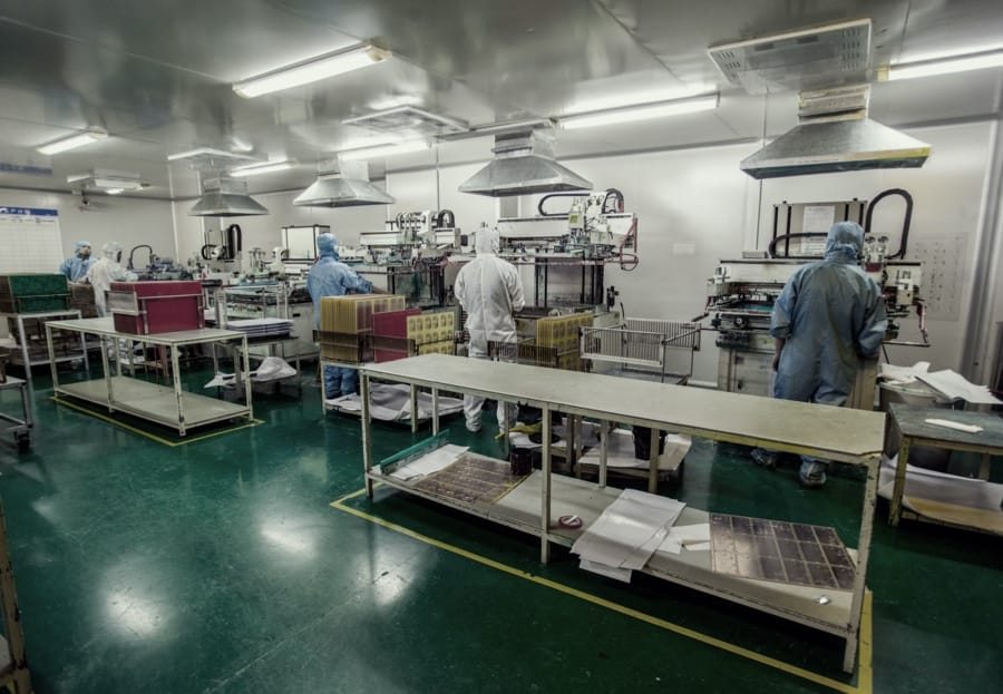
Every stage of PCB fabrication, including layer stackup, photolithography, drilling, plating, surface finish, and electrical testing, is performed at our ISO-certified factories in Shenzhen and Jiangmen.
This ensures complete traceability, lead time consistency (standard: 5 to 6 days; expedited: 24 to 48 hours), and quality oversight for PCBs up to 64 layers and 40:1 aspect ratio.

Certified to Global Standards
WellPCB is certified to ISO 9001:2015 (Quality Management), ISO 14001:2015 (Environmental), ISO 13485:2016 (Medical), and IATF 16949:2016 (Automotive), with UL-listed PCBs manufactured to IPC-6012 and IPC-A-600 Class 2 and Class 3 standards.
All PCBs are RoHS and REACH compliant.

True One-Stop Electronic Manufacturing
Our services go beyond fabrication.
We include SMT/through-hole PCB assembly (BGA/QFN to 0.2 mm pitch), full turnkey sourcing from authorized distributors (Mouser, Digi-Key, Arrow), custom wire harnesses, firmware programming, flying probe and functional testing, and full box build assembly.

Transparent Quoting & No Hidden Costs
Get instant quotes based on exact technical specifications, layer count, surface finish, copper weight, solder mask color, board thickness, etc.
We support multi-currency payments (USD, EUR, AUD), and guarantee no surprise charges during high-mix or HDI production runs.

Engineering-Grade Technical Support
Our support team includes PCB design-for-manufacturing (DFM) experts, stackup planners, and SMT process engineers who assist with Gerber, BOM, and stencil file review.
We identify manufacturability risks (eg. solder mask clearance, via annular ring violations) before production begins.

Rapid Prototyping with Scale-Up Continuity
Prototype from a single unit to mass production (up to 10,000+ boards) using the same tested process chain.
All boards are built with consistent documentation, testing, and quality checkpoints to ensure functional and dimensional consistency throughout your product lifecycle.
Our PCB Manufacturing Process
We manufacture various custom wiring harnesses engineered to meet the electrical, environmental, and mechanical demands of specialized applications across multiple industries.
1
Gerber Review & CAM Optimization
All incoming Gerber files undergo Design for Manufacturability (DFM) checks and CAM engineering, including layer alignment, drill/rout verification, netlist integrity checks, soldermask clearance review, and impedance modeling.
2
Inner Layer Imaging & Etching
Photoresist imaging uses LDI (Laser Direct Imaging) systems to define inner-layer copper patterns. Etching removes exposed copper, achieving line/space resolutions as tight as 1.8 mil.
3
AOI for Inner Layers
Automated Optical Inspection (AOI) detects short/open circuits, line width variations, and registration defects on each inner layer prior to lamination, ensuring early defect containment.
4
Multilayer Lamination with Prepreg
Layer stackups are consolidated using high-Tg FR4 or specialty prepreg under controlled pressure/temperature cycles. Up to 64 layers are supported, with impedance-controlled dielectric thickness targeting ±10%.
5
Drilling (Mechanical/Laser)
High-precision CNC drills (±0.025 mm accuracy) form through-holes and vias down to 0.08 mm. For HDI boards, CO₂/UV laser drilling enables stacked microvias, blind/buried vias, and via-in-pad structures.
6
Electroless Copper Deposition
A catalytic copper layer is chemically deposited to create a conductive base in all hole walls. This seed layer is essential for ensuring uniform subsequent electrolytic plating.
7
Outer Layer Pattern Plating
Electrolytic copper plating is performed with controlled current density (20 to 30 ASF) to thicken traces and via barrels. Nickel/gold plating may also be applied to selected areas.
8
Outer Layer Etching
Outer layers are developed using photolithography and etching to define final circuit patterns. All conductive paths are verified against the netlist and CAM data.
9
Soldermask Application
Liquid photoimageable (LPI) soldermask is screen-coated or spray-applied, then UV-imaged and developed to expose pads and vias. Supported colors include green, black, blue, white, yellow, and matte options.
10
Surface Finish Deposition
Surface finishes such as ENIG, ENEPIG, HASL (leaded/lead-free), OSP, immersion silver, and tin are applied to exposed pads. These finishes ensure solderability and long-term oxidation resistance.
11
Silkscreen Printing
High-resolution legend ink is printed using screen or inkjet methods, with white, yellow, or black options. Line widths down to 4 mil ensure clear component identification.
12
100% Electrical Testing
All boards undergo electrical testing via flying probe or bed-of-nails to verify netlist compliance, continuity, and isolation. High-voltage and high-resistance leakage testing can be applied for Class 3 builds.
13
Profiling, V-Scoring, Routing
PCBs are separated using mechanical routing, V-score, or punch tooling. Profiling tolerance is maintained at ±0.04 mm to match mechanical enclosure requirements.
14
Visual QA Inspection
Final visual inspection checks for soldermask integrity, surface finish consistency, silkscreen legibility, and board edge quality. IPC-A-600 criteria guide acceptance levels.
15
Anti-Static Packaging
Boards are vacuum-sealed in anti-static packaging with desiccant packs and humidity indicators. Panel or single-unit packaging is available per order specs.
16
Certified Delivery & Documentation
Each shipment includes test reports, CoC (Certificate of Conformance), dimensional inspection results, and RoHS/REACH compliance documentation as required.
Industries We Serve As a PCB Manufacturer
WellPCB supplies printed circuit boards to various technology-driven industries with distinct electrical, mechanical, and environmental requirements. Our in-house PCB fabrication and assembly services are built to meet strict regulatory, performance, and lifecycle standards, from impedance-critical RF boards to rugged, thermally-managed automotive PCBs.

Automotive & EV
We manufacture automotive-grade printed circuit boards with copper weights up to 20 oz for high-current applications.
All builds conform to IPC-6012 Class 3 standards with validated thermal cycling resistance and high aspect ratio vias, supporting operational reliability in power converters, battery management systems, and control modules.

Telecom & RF
High-frequency PCBs are fabricated using Rogers RO4003 and RO4350 laminates with tight impedance control (±5 Ω or better).
Supported features include low-loss signal routing, differential pair tuning, and microstrip geometry for antenna and RF front-end modules in communication equipment.
Aerospace / Defense
Rigid-flex PCB capabilities support aerospace navigation, avionics, and embedded defense systems.
We offer multi-layer flex construction with stacked microvias, blind and buried vias, and conformal coating options.
Edge contact features such as hard gold plating and compliance with IPC-Class 3 standards ensure performance in mission-critical environments.
Medical Devices
Our ISO 13485:2016 certified processes support the fabrication of PCBs for diagnostic, imaging, and patient monitoring systems.
We offer impedance-controlled stackups, AOI inspection, X-ray validation for fine-pitch components, and optional conformal coatings for medical-grade protection.
Industrial Controls
For automation, robotics, and motor control, we provide PCBs with 12+ layer HDI stackups, via-in-pad construction, and surface finishes like ENIG and OSP.
All materials meet UL 94V-0 flammability requirements and support environmental durability in industrial-grade enclosures.
Consumer Electronics
We support high-volume and prototype production of LED boards, wearables, and embedded control units.
Available options include aluminum-core PCBs for efficient thermal dissipation, low-cost FR4 builds, and multi-color soldermask and legend customization for device branding and user interface.
How to Order Your PCB
in 5 Easy Steps
PCB Manufacturing and Order Review Process

Submit Your PCB Design
Upload your Gerber files or use our easy online PCB design tool to create your board layout. Make sure your files are complete and correctly formatted to ensure smooth processing and production accuracy.

Select Your PCB Specifications
Customize your order by choosing the technical specifications—number of layers, board dimensions, thickness, copper weight, solder mask color, surface finish, and more. Our intuitive interface helps you configure everything based on your project’s needs.

Get an Instant Quote
Once your design and specs are in place, you'll receive a transparent, instant quote. Pricing updates in real time as you modify options, so you can adjust your selections to match your budget before placing the order.

Confirm Order & Make Payment
Review your entire order for accuracy, including file previews and selected specs. After confirmation, proceed to secure checkout and choose your preferred payment method. You’ll receive an email confirmation with order details.

Production & Delivery
Your PCB moves into production immediately. We’ll keep you updated throughout the manufacturing process. Once completed, your boards are carefully packed and shipped to your door, with tracking information provided for your convenience.
All Circuit Boards and Assembly Services
WellPCB is trusted by millions of
businesses and innovators.
Why Choose WellPCB?
WellPCB stands out among USA PCB manufacturers by delivering superior quality, advanced solutions, and unmatched reliability. With years of experience serving global markets, WellPCB has earned a reputation as one of the top PCB manufacturers in USA.
WellPCB specializes in multilayer PCBs for advanced electronic applications. You can order these boards with $100 off using our special offer, providing high complexity at competitive rates for demanding projects.

Hommer Zhao
Founder and Chief Editor – Hommer Zhao
Welcome! I’m Hommer Zhao, the founder and Chief Editor of WellPCB. With years of experience in the PCB industry, I’m committed to making sure our content is both accurate and helpful. We’re proud to serve a growing community of over 4,000 customers worldwide, and our goal is to provide you with the best resources and support. Your satisfaction is our top priority, and we’re here to help you every step of the way!

Jesse Holland
Technical Manager – Jesse Holland
Hi, I’m Jesse Holland, an Engineer and Technical Manager at WellPCB. With years of experience in PCB design and engineering, I’m here to ensure that every project we work on meets the highest technical standards. I lead our team, focusing on precision and innovation, collaborating closely with clients to provide tailored solutions and expert guidance. Whether you’re facing a complex design challenge or need advice on technical aspects, I’m here to ensure your project is a success from start to finish.

Nathan Jensen
Purchasing Manager – Nathan Jensen
Hi, I’m Nathan Jenson, the Purchasing Manager at WellPCB. I’m responsible for sourcing the best materials and components to ensure our products meet the highest quality standards. With my extensive experience in procurement, I work closely with suppliers to secure reliable and cost-effective solutions while maintaining strong relationships to support our operations. I aim to ensure every project runs smoothly by providing the resources needed to deliver on time and to your satisfaction.

Emma
Sales Manager – Emma
Hey, I am Emma, sales manager at WellPCB. I studied electronic science and technology at university and have served customers for PCB and PCB Assembly service for several years.
I enjoy communicating with customers and our technicians to solve problems, and customers always say, "It's great to have you onboard".
It is my pleasure and honour to be helpful. Contact me now, and you'll know.

Bella and Cassiel
Sales Representatives – Bella and Cassiel
We’re Bella and Cassiel, your dedicated sales representatives at WellPCB. With our extensive knowledge of the PCB industry, we’re here to provide exceptional service and support. We take the time to understand your unique needs and are always ready to offer tailored solutions and advice. Whether you need product recommendations, assistance with your orders, or simply have a question, we’re here to ensure your experience is smooth and seamless at every step.

Mandy and Wendy
Sales Representatives – Mandy and Wendy
We’re Mandy and Wendy, your friendly sales representatives at WellPCB. Passionate about helping our customers, we bring a wealth of experience in the PCB industry to provide you with the best solutions and service. We take pride in building strong relationships with our clients, understanding their specific needs, and offering personalised support to ensure their satisfaction. Whether you’re looking for advice, product information, or assistance with any part of your order, we’re here to make your experience as smooth and efficient as possible.
Our Team
Our skilled engineers and technicians bring expertise and precision to every PCB assembly project. Committed to quality, efficiency, and innovation, our team ensures every order meets the highest UL, IPC, ROHS & REACH standards, delivering reliable solutions tailored to your needs.
- Founder and Chief Editor – Hommer Zhao
- Technical Manager – Jesse Holland
- Purchasing Manager – Nathan Jensen
- Sales Manager – Emma
- Sales Representatives – Bella and Cassiel
- Sales Representatives – Mandy and Wendy
Our PCB Manufacturer Case Studies
Case Study
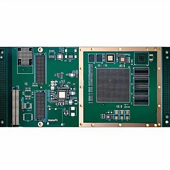
16-Layer HDI PCB for High-Speed Electronic Systems
This 16-layer HDI (High-Density Interconnect) PCB is designed for complex electronic systems requiring high-speed signal transmission, dense interconnect routing, and multi-level via structures. It supports ultra-fine trace geometry and advanced stacked via architecture, ideal for applications like network equipment, AI computing boards, and advanced medical or aerospace electronics.
Product Specifications:
- Board Type: 16-layer HDI PCB
- Board Thickness: 1.8 mm
- Inner Layer Spacing: 0.127 mm (127 µm)
- Via Structure: L1–2, L2–3, L1–3, L2–7, L2–15, L15–16
- Line Width / Line Space: 0.076 / 0.076 mm (≈3 mil / 3 mil)
- Material: High-speed/low-loss laminate (e.g., Megtron 6, Isola I-Speed, etc.)
- Copper Thickness: Typically ½ oz inner, 1 oz outer (customizable)
- Surface Finish: ENIG / OSP / Immersion Silver (varies by application)
- Impedance Control: Yes (±10% tolerance for differential pairs)
- Application: AI, servers, data centers, telecom, aerospace
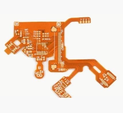
Case Study
ENIG LCD Connector Flex Circuit Board
This project involves a high-precision multi-layer flexible board developed for use in LCD connectors, focusing on flexibility, signal integrity, and mechanical durability for the flexible connector interface in electronic devices like LCD screens. It includes a multi-layer structure with precise surface finishes and materials to support high-frequency signals while maintaining flexibility and reliability.
Product Specifications:
Material Structure:
- Double-sided adhesive
- Low-loss yellow covering film
- Core buildup: (line copper + glue + high-frequency medium polyimide base material + glue + line copper)
- Outer layers: Low-loss yellow covering film
- Flexibility Requirements: Designed for free bending and winding
- Positional Accuracy (Male Component): ±0.03 mm tolerance
- Thickness: 0.15 mm
- Reinforcement: Front and back reinforced with 0.15 mm steel sheets
Manufacturing Processes:
- Solder coating
- Plug plating
- Covering layer application
- Film-covered type assembly
- Resistance and welding type shielding torsion
- Surface Treatment: ENIG (Electroless Nickel Immersion Gold, 1 to 2 microinches)
- Minimum Line Width / Spacing: 0.06 mm / 0.09 mm
- Application: Connector components for LCD modules
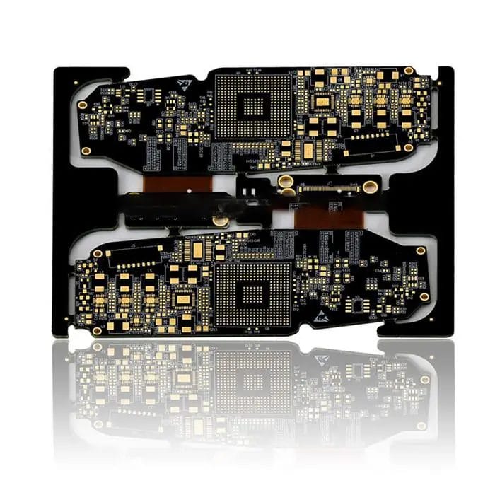
Case Study
10-Layer Rigid-Flex PCB for Smartphone Mainboard
This 10-layer rigid-flex PCB is engineered for smartphone motherboards, integrating high-density routing, multiple interconnects, and flexible sections for space-saving, compact, and lightweight device architecture. Designed for advanced mobile electronics, it offers excellent signal integrity, fine-line capabilities, and durability under thermal and mechanical stress.
Product Specifications:
- Board Type: 10-layer rigid-flex PCB
- Total Thickness: 1.5 mm
- Line Width / Line Space: 3 mil / 4 mil (≈75 µm / 100 µm)
- Solder Bridge Width: 5 mil (≈125 µm)
- Flexible Layers: Polyimide (PI) with rolled annealed copper
- Rigid Layers: FR-4 (high Tg, halogen-free optional)
- Via Type: Blind and buried via (optional for HDI)
- Application: Smartphone motherboards, display drivers, power modules
Client Feedback About Our PCB Manufacturer Services
![]()

As an R&D manager, I have had an outstanding experience working with WELL-PCB. For many years, our company has entrusted them with the production, assembly, and programming of the boards developed in our R&D unit, and they have consistently exceeded our expectations.
![]()
Hamid Reza Moshayedi
R&D Manager
![]()
Their work is very impressively perfect. Today, when they check our company PCB board after assemble. They found a fake short point which many engineers has never found in the past years. But that is just designed so. The PCB board quality is excellent. Their service is also excellent.

MikeZ
![]()
My friend introduced WellPCB to me, the first try, a little look forward to. I ordered a 47*72 10ps PCB, and I can’t wait to receive my PCB. So I used expedited service and received my PCB in three days. I tested and soldered the PCB, Quality is really good, silkscreen, plating also great.

Warren Cliton
PCB Manufacturer FAQs
Do you provide IPC Class 3 boards?
Yes, we support IPC Class 2 and Class 3 production standards, including inspection protocols and documentation for high-reliability applications.
What is your copper capacity?
We offer finished copper thicknesses up to 1000 μm (approximately 28 oz), supporting high-current and power distribution needs.
Get $100 Off Your First Order with a World-Class
PCB Manufacturer
Partner with WellPCB for high-quality PCB prototype and fabrication services backed by full in-house control, global compliance, and engineering-grade precision. Whether you need a single prototype or a production-scale run, we’re ready to deliver.

Your Trusted PCB Manufacturer & Wiring Harness Provider
Get $100 Off Your First Order!
High-Quality PCB Manufacturing, Assembly & Wiring Harness Services
Fast Turnaround & Reliable Service

WellPCB. All rights reserved