Manage How HDL Coder Maps RAM - MATLAB & Simulink (original) (raw)
You can manage how HDL Coder™ maps design elements to RAM by using the RAM mapping threshold model configuration parameter and the Specify vector input access block parameter of RAM System blocks.
Specify Minimum RAM Mapping Threshold
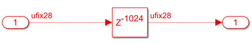
You can map delays or persistent arrays that are greater than a threshold bit size to RAM by using the model configuration parameter RAM mapping threshold. For example, if your design contains a Delay block with a delay length of 1024 cycles and a word length of 28 bits and you set the HDL block propertyUseRAM to on and the RAM mapping threshold parameter to 256 total bits, the total RAM size of the Delay block, 28672 bits, exceeds the threshold. HDL Coder maps 1024x28 bits to the RAM on hardware. To calculate the total RAM size, use this formula:
RAMSize = Delay length * Word length * Vector length * Complexity
In this case, the input vector length is 1 and the complexity of a real data type is 1, so the total RAM size equation is:
RAMSize = Delay length * Word length = 1024*28
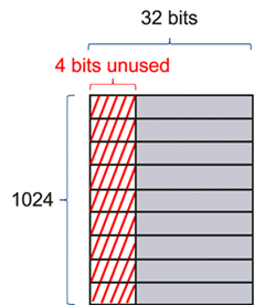
With a block RAM (BRAM) size on the target hardware of 1024x32 bits, HDL Coder maps the delay with 4 bits of unused width for each row of RAM. As a result, depending on the shape of the data defined by delay length and word length, the RAM mapping might be inefficient.
RAM Merging
RAM merging is a process that merges several delays and maps them to RAM together. During HDL code generation, RAM merging occurs when you have multiple Delay blocks with the same delay length in the same subsystem. RAM merging fuses the delays into a single delay that has a RAM size equal to the sum of the original RAM sizes. If this new RAM size is greater than the RAM mapping threshold value, HDL Coder maps the merged delays to RAM. For example, consider a subsystem with three Delay blocks, where each Delay block has a total RAM size of 40 bits. If the RAM mapping threshold is 100, all three delays map to RAM because they have a total of 3x40=120 bits when they merge.
Exclude Inefficient RAM Mapping
To exclude delays or persistent arrays that map inefficiently to RAM, you can define thresholds for:
- The delay length of delays or the array size of persistent array variables
- The word length or bit width of the data type
Use these thresholds to selectively map data that has a shape similar to specific block RAM configuration on your target hardware.
Set Total RAM Size for RAM Mapping Threshold
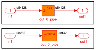
For example, consider this model, which has a DUT that contains two subsystems. If the RAM mapping threshold is256, HDL Coder maps both of these subsystems in the DUT in the generated model to block RAM on the Xilinx® RAMB36E1, because both subsystems contain delays with a total bit size of 32768 bits, which is greater than the threshold, even with different delay lengths and bit widths.
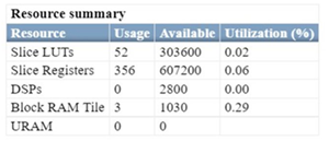
To determine how many block RAMs the design uses, run synthesis on the model. For more information, see HDL Code Generation and FPGA Synthesis from Simulink Model. This is the resource summary report from synthesis:
You can configure the BRAM on the Xilinx RAMB36E1 for sizes of 512x64 bits or 1024x32 bits. The first subsystem inefficiently maps to block RAM and takes up two BRAM of size 512x64 bits, while the second subsystem maps more efficiently to one BRAM of size 1024x32 bits.
Set Delay Length and Word Length for RAM Mapping Threshold
Suppose that you change the RAM mapping threshold parameter in the previous example to 1024x1, where 1024 is the delay length threshold and 1 is the word length threshold. To determine how many block RAMs the design uses, run synthesis on the model. This is the resource summary report from synthesis:
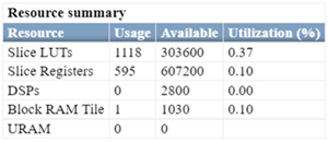
Now, only the second subsystem maps to BRAM, because the first subsystem has a delay length of 256 cycles, which is less than the delay length threshold of 1024. As a result, the design uses only one BRAM to map the second subsystem. The first subsystem maps to LUTs and registers.
Control Vector Input Handling for RAM System Blocks
Since R2025a
You can select serial access or parallel access for RAM systems by setting theSpecify vector input access block parameter of a RAM System block or by setting the VectorAccess property of the hdl.RAM System object™.
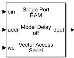
Use parallel access to infer parallel banks of RAM from vector inputs to RAM System blocks. Use serial access to design systems that can reconfigure lookup operations after hardware deployment.