p–i–n photodiodes (original) (raw)
Definition: photodiodes with a p–i–n semiconductor structure
Alternative term: PIN photodiodes
 photonic devices
- photodetectors
- photodiodes
* avalanche photodiodes
* Geiger mode photodiodes
* lateral effect photodiodes
* quadrant photodiodes
* p–i–n photodiodes
* silicon photodiodes
* germanium photodiodes
* InGaAs and GaAs photodiodes
* photodiode arrays
* (more topics)
- photodiodes
Related: photodiodesmetal–semiconductor–metal photodetectors
Page views in 12 months: 3382
DOI: 10.61835/zis Cite the article: BibTex BibLaTex plain textHTML Link to this page! LinkedIn
Content quality and neutrality are maintained according to our editorial policy.
📦 For purchasing p–i–n photodiodes, use the RP Photonics Buyer's Guide — an expert-curated directory for finding all relevant suppliers, which also offers advanced purchasing assistance.
Contents
What are p–i–n Photodiodes?
A p–i–n photodiode, also called PIN photodiode, is a common type of photodiode with an intrinsic (i) (i.e., undoped) region between the n- and p-doped regions. Most of the photons are absorbed in the intrinsic region, and carriers generated therein can efficiently contribute to the photocurrent. In Figure 1, the electrodes are shown in black: the cathode is a flat electrode, whereas the anode has the form of a ring (of which two opposite parts are seen in the shown cross-section). The positive pole of the (reverse) bias voltage is connected to the cathode. On top of the p region, there is an anti-reflection coating.
Advantages of the p–i–n Design

Figure 1: Schematic drawing of a p–i–n photodiode. The green layer is an anti-reflection coating.
Ordinary p–n photodiodes can suffer from the following problems:
- The width of the depletion region may be well below the absorption length, so that only some fraction of the generated photocarriers are generated within the depletion region. The collection of the carriers generated outside the depletion region may be limited, leading to a reduced quantum efficiency.
- Even for those carriers generated outside the depletion region which eventually diffuse into the depletion region and can thus contribute to the photocurrent, that diffusion takes some time; that results in a tail in the impulse response function, which can limit the detection bandwidth.
These problems can be mitigated or avoided with p–i–n photodiode design. There, most carriers are generated in the intrinsic region because that can be much thicker than the depletion region of a p–n structure. Another effect of the thick intrinsic region can be the reduced capacitance, which allows for a higher detection bandwidth.
Some p–i–n diodes are made from different semiconductor materials, where the band gap energy is below the photon energy only for the intrinsic region, but not for the p and n regions. In that case, any absorption outside the intrinsic region can be avoided.
The fastest p–i–n photodiodes have bandwidths well above 100 GHz. Their active areas typically have a diameter of only a few microns. They are often made in fiber-coupled form and can be applied e.g. in receivers for optical fiber communications; the achieved bit rates can be as high as 160 Gbit/s.
Materials for p–i–n Photodiodes
Some p–i–n diodes are based on silicon. They are sensitive throughout the visible spectral region and in the near infrared up to ≈ 1 μm. At longer wavelengths, the absorption efficiency and thus the responsivity drops sharply, but the parameters of that cut-off depend on the thickness of the intrinsic region.
For longer wavelengths up to ≈ 1.7 μm (or with extended spectral response up to 2.6 μm), InGaAs p–i–n diodes are available, although at significantly higher prices (particularly for large active areas). Small InGaAs photodiodes can be extremely fast.
Germanium p–i–n diodes can be a cheaper alternative to InGaAs diodes, but they have a much slower response and exhibit a much larger dark current.
Frequently Asked Questions
This FAQ section was generated with AI based on the article content and has been reviewed by the article’s author (RP).
What is a p–i–n photodiode?
A p–i–n photodiode is a type of photodiode which has an intrinsic (i.e., undoped) semiconductor region located between the p-doped and n-doped regions. This intrinsic layer is where most photons are absorbed.
What are the main advantages of the p–i–n photodiode design?
Compared to a simple p–n photodiode, the p–i–n design's thick intrinsic region allows for more efficient absorption of light, leading to a higher quantum efficiency. It also enables a faster response and a reduced capacitance, which both contribute to a higher detection bandwidth.
How does the intrinsic layer improve the photodiode's speed?
Most charge carriers are generated within the thick intrinsic region, where a strong electric field quickly sweeps them to the electrodes. This avoids the slow process of carrier diffusion from outside the depletion region, which can limit the speed of ordinary p–n photodiodes.
What semiconductor materials are used to make p–i–n photodiodes?
Silicon is commonly used for detecting visible and near-infrared light up to about 1 μm. For longer infrared wavelengths up to 1.7 μm or more, InGaAs is often used, while germanium serves as a lower-cost, lower-performance alternative.
Suppliers
Sponsored content: The RP Photonics Buyer's Guide contains 14 suppliers for p–i–n photodiodes. Among them:

⚙ hardware
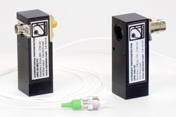
Very fast rise time p–i–n photodiodes for measurement of optical waveforms with rise times starting from 10 ps and spectral coverage from 170 to 2600 nm (VUV to IR) have bandwidths from DC up to 30 GHz. Configurations include free-space, fiber receptacle or SM-fiber-pigtailed options and have compact metal housings for noise immunity. The UV-extended versions of the Si photodiodes are the only commercial products that cover the spectral range from 170 to 1100 nm with a rise time < 50 ps. For maximum flexibility, most models are not internally terminated. A 50 Ohm external termination supports the highest speed operation and a high impedance load generates large amplitude signals. Applications include pulse form and duration measurement, laser synchronization, mode beating monitoring and heterodyne measurements. Balanced photodiodes complement the large selection of models.
Questions and Comments from Users
Here you can submit questions and comments. As far as they get accepted by the author, they will appear above this paragraph together with the author’s answer. The author will decide on acceptance based on certain criteria. Essentially, the issue must be of sufficiently broad interest.
Please do not enter personal data here. (See also our privacy declaration.) If you wish to receive personal feedback or consultancy from the author, please contact him, e.g. via e-mail.
By submitting the information, you give your consent to the potential publication of your inputs on our website according to our rules. (If you later retract your consent, we will delete those inputs.) As your inputs are first reviewed by the author, they may be published with some delay.