NVIDIA Ampere Architecture In-Depth (original) (raw)
Today, during the 2020 NVIDIA GTC keynote address, NVIDIA founder and CEO Jensen Huang introduced the new NVIDIA A100 GPU based on the new NVIDIA Ampere GPU architecture. This post gives you a look inside the new A100 GPU, and describes important new features of NVIDIA Ampere architecture GPUs.
The diversity of compute-intensive applications running in modern cloud data centers has driven the explosion of NVIDIA GPU-accelerated cloud computing. Such intensive applications include AI deep learning (DL) training and inference, data analytics, scientific computing, genomics, edge video analytics and 5G services, graphics rendering, cloud gaming, and many more. From scaling-up AI training and scientific computing, to scaling-out inference applications, to enabling real-time conversational AI, NVIDIA GPUs provide the necessary horsepower to accelerate numerous complex and unpredictable workloads running in today’s cloud data centers.
NVIDIA GPUs are the leading computational engines powering the AI revolution, providing tremendous speedups for AI training and inference workloads. In addition, NVIDIA GPUs accelerate many types of HPC and data analytics applications and systems, allowing you to effectively analyze, visualize, and turn data into insights. The NVIDIA accelerated computing platforms are central to many of the world’s most important and fastest-growing industries.
Introducing the NVIDIA A100 Tensor Core GPU
The NVIDIA A100 Tensor Core GPU is based on the new NVIDIA Ampere GPU architecture, and builds upon the capabilities of the prior NVIDIA Tesla V100 GPU. It adds many new features and delivers significantly faster performance for HPC, AI, and data analytics workloads.
A100 provides strong scaling for GPU compute and DL applications running in single– and multi-GPU workstations, servers, clusters, cloud data centers, systems at the edge, and supercomputers. The A100 GPU enables building elastic, versatile, and high throughput data centers.
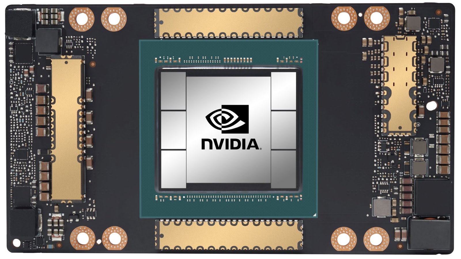
Figure 1. NVIDIA A100 GPU on the new SXM4 module.
The A100 GPU includes a revolutionary new multi-instance GPU (MIG) virtualization and GPU partitioning capability that is particularly beneficial to cloud service providers (CSPs). When configured for MIG operation, the A100 permits CSPs to improve the utilization rates of their GPU servers, delivering up to 7x more GPU Instances for no additional cost. Robust fault isolation allows them to partition a single A100 GPU safely and securely.
A100 adds a powerful new third-generation Tensor Core that boosts throughput over V100 while adding comprehensive support for DL and HPC data types, together with a new Sparsity feature that delivers a further doubling of throughput.
New TensorFloat-32 (TF32) Tensor Core operations in A100 provide an easy path to accelerate FP32 input/output data in DL frameworks and HPC, running 10x faster than V100 FP32 FMA operations or 20x faster with sparsity. For FP16/FP32 mixed-precision DL, the A100 Tensor Core delivers 2.5x the performance of V100, increasing to 5x with sparsity.
New Bfloat16 (BF16)/FP32 mixed-precision Tensor Core operations run at the same rate as FP16/FP32 mixed-precision. Tensor Core acceleration of INT8, INT4, and binary round out support for DL inferencing, with A100 sparse INT8 running 20x faster than V100 INT8. For HPC, the A100 Tensor Core includes new IEEE-compliant FP64 processing that delivers 2.5x the FP64 performance of V100.
The NVIDIA A100 GPU is architected to not only accelerate large complex workloads, but also efficiently accelerate many smaller workloads. A100 enables building data centers that can accommodate unpredictable workload demand, while providing fine-grained workload provisioning, higher GPU utilization, and improved TCO.
The NVIDIA A100 GPU delivers exceptional speedups over V100 for AI training and inference workloads as shown in Figure 2. Similarly, Figure 3 shows substantial performance improvements across different HPC applications.
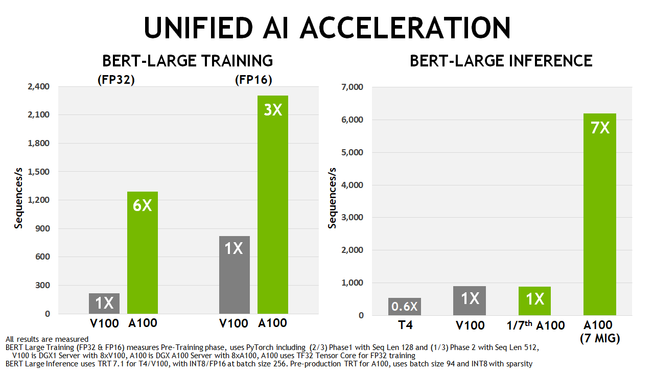
Figure 2. A100 GPU performance in BERT deep learning training and inference scenarios compared to NVIDIA Tesla V100 and NVIDIA Tesla T4.
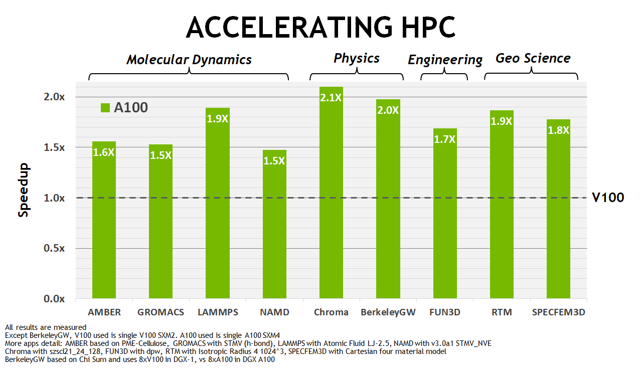
Figure 3. A100 GPU HPC application speedups compared to NVIDIA Tesla V100.
Key features
Fabricated on the TSMC 7nm N7 manufacturing process, the NVIDIA Ampere architecture-based GA100 GPU that powers A100 includes 54.2 billion transistors with a die size of 826 mm2.
A100 GPU streaming multiprocessor
The new streaming multiprocessor (SM) in the NVIDIA Ampere architecture-based A100 Tensor Core GPU significantly increases performance, builds upon features introduced in both the Volta and Turing SM architectures, and adds many new capabilities.
The A100 third-generation Tensor Cores enhance operand sharing and improve efficiency, and add powerful new data types, including the following:
- TF32 Tensor Core instructions that accelerate processing of FP32 data
- IEEE-compliant FP64 Tensor Core instructions for HPC
- BF16 Tensor Core instructions at the same throughput as FP16
| Peak FP641 | 9.7 TFLOPS |
|---|---|
| Peak FP64 Tensor Core1 | 19.5 TFLOPS |
| Peak FP321 | 19.5 TFLOPS |
| Peak FP161 | 78 TFLOPS |
| Peak BF161 | 39 TFLOPS |
| Peak TF32 Tensor Core1 | 156 TFLOPS | 312 TFLOPS2 |
| Peak FP16 Tensor Core1 | 312 TFLOPS | 624 TFLOPS2 |
| Peak BF16 Tensor Core1 | 312 TFLOPS | 624 TFLOPS2 |
| Peak INT8 Tensor Core1 | 624 TOPS | 1,248 TOPS2 |
| Peak INT4 Tensor Core1 | 1,248 TOPS | 2,496 TOPS2 |
Table 1. A100 Tensor Core GPU performance specs.
1) Peak rates are based on the GPU boost clock.
2) Effective TFLOPS / TOPS using the new Sparsity feature.
New Sparsity support in A100 Tensor Cores can exploit fine-grained structured sparsity in DL networks to double the throughput of Tensor Core operations. Sparsity features are described in detail in the A100 introduces fine-grained structured Sparsity section later in this post.
The larger and faster L1 cache and shared memory unit in A100 provides 1.5x the aggregate capacity per SM compared to V100 (192 KB vs. 128 KB per SM) to deliver additional acceleration for many HPC and AI workloads.
Several other new SM features improve efficiency and programmability and reduce software complexity.
40 GB HBM2 and 40 MB L2 cache
To feed its massive computational throughput, the NVIDIA A100 GPU has 40 GB of high-speed HBM2 memory with a class-leading 1555 GB/sec of memory bandwidth—a 73% increase compared to Tesla V100. In addition, the A100 GPU has significantly more on-chip memory including a 40 MB Level 2 (L2) cache—nearly 7x larger than V100—to maximize compute performance. With a new partitioned crossbar structure, the A100 L2 cache provides 2.3x the L2 cache read bandwidth of V100.
To optimize capacity utilization, the NVIDIA Ampere architecture provides L2 cache residency controls for you to manage data to keep or evict from the cache. A100 also adds Compute Data Compression to deliver up to an additional 4x improvement in DRAM bandwidth and L2 bandwidth, and up to 2x improvement in L2 capacity.
Multi-Instance GPU
The new Multi-Instance GPU (MIG) feature allows the A100 Tensor Core GPU to be securely partitioned into as many as seven separate GPU Instances for CUDA applications, providing multiple users with separate GPU resources to accelerate their applications.
With MIG, each instance’s processors have separate and isolated paths through the entire memory system. The on-chip crossbar ports, L2 cache banks, memory controllers, and DRAM address busses are all assigned uniquely to an individual instance. This ensures that an individual user’s workload can run with predictable throughput and latency, with the same L2 cache allocation and DRAM bandwidth, even if other tasks are thrashing their own caches or saturating their DRAM interfaces.
MIG increases GPU hardware utilization while providing a defined QoS and isolation between different clients, such as VMs, containers, and processes. MIG is especially beneficial for CSPs who have multi-tenant use cases. It ensures that one client cannot impact the work or scheduling of other clients, in addition to providing enhanced security and allowing GPU utilization guarantees for customers.
Third-generation NVIDIA NVLink
The third-generation of NVIDIA high-speed NVLink interconnect implemented in A100 GPUs and the new NVIDIA NVSwitch significantly enhances multi-GPU scalability, performance, and reliability. With more links per GPU and switch, the new NVLink provides much higher GPU-GPU communication bandwidth, and improved error-detection and recovery features.
Third-generation NVLink has a data rate of 50 Gbit/sec per signal pair, nearly doubling the 25.78 Gbits/sec rate in V100. A single A100 NVLink provides 25-GB/second bandwidth in each direction similar to V100, but using only half the number of signal pairs per link compared to V100. The total number of links is increased to 12 in A100, vs. 6 in V100, yielding 600 GB/sec total bandwidth vs. 300 GB/sec for V100.
Support for NVIDIA Magnum IO and Mellanox interconnect solutions
The A100 Tensor Core GPU is fully compatible with NVIDIA Magnum IO and Mellanox state-of-the-art InfiniBand and Ethernet interconnect solutions to accelerate multi-node connectivity.
The Magnum IO API integrates computing, networking, file systems, and storage to maximize I/O performance for multi-GPU, multi-node accelerated systems. It interfaces with CUDA-X libraries to accelerate I/O across a broad range of workloads, from AI and data analytics to visualization.
PCIe Gen 4 with SR-IOV
The A100 GPU supports PCI Express Gen 4 (PCIe Gen 4), which doubles the bandwidth of PCIe 3.0/3.1 by providing 31.5 GB/sec vs. 15.75 GB/sec for x16 connections. The faster speed is especially beneficial for A100 GPUs connecting to PCIe 4.0-capable CPUs, and to support fast network interfaces, such as 200 Gbit/sec InfiniBand.
A100 also supports single root input/output virtualization (SR-IOV), which allows sharing and virtualizing a single PCIe connection for multiple processes or VMs.
Improved error and fault detection, isolation, and containment
It is critically important to maximize GPU uptime and availability by detecting, containing, and often correcting errors and faults, rather than forcing GPU resets. This is especially true in large multi-GPU clusters and single-GPU, multi-tenant environments such as MIG configurations. The A100 Tensor Core GPU includes new technology to improve error/fault attribution, isolation, and containment as described in the in-depth architecture sections later in this post.
Asynchronous copy
The A100 GPU includes a new asynchronous copy instruction that loads data directly from global memory into SM shared memory, eliminating the need for intermediate register file (RF) usage. Async-copy reduces register file bandwidth, uses memory bandwidth more efficiently, and reduces power consumption. As the name implies, asynchronous copy can be done in the background while the SM is performing other computations.
Asynchronous barrier
The A100 GPU provides hardware-accelerated barriers in shared memory. These barriers are available using CUDA 11 in the form of ISO C++-conforming barrier objects. Asynchronous barriers split apart the barrier arrive and wait operations and can be used to overlap asynchronous copies from global memory into shared memory with computations in the SM. They can be used to implement producer-consumer models using CUDA threads. Barriers also provide mechanisms to synchronize CUDA threads at different granularities, not just warp or block level.
Task graph acceleration
CUDA task graphs provide a more efficient model for submitting work to the GPU. A task graph consists of a series of operations, such as memory copies and kernel launches, connected by dependencies. Task graphs enable a define-once and run-repeatedly execution flow. A predefined task graph allows the launch of any number of kernels in a single operation, greatly improving application efficiency and performance. A100 adds new hardware features to make the paths between grids in a task graph significantly faster.
A100 GPU hardware architecture
The NVIDIA GA100 GPU is composed of multiple GPU processing clusters (GPCs), texture processing clusters (TPCs), streaming multiprocessors (SMs), and HBM2 memory controllers.
The full implementation of the GA100 GPU includes the following units:
- 8 GPCs, 8 TPCs/GPC, 2 SMs/TPC, 16 SMs/GPC, 128 SMs per full GPU
- 64 FP32 CUDA Cores/SM, 8192 FP32 CUDA Cores per full GPU
- 4 third-generation Tensor Cores/SM, 512 third-generation Tensor Cores per full GPU
- 6 HBM2 stacks, 12 512-bit memory controllers
The A100 Tensor Core GPU implementation of the GA100 GPU includes the following units:
- 7 GPCs, 7 or 8 TPCs/GPC, 2 SMs/TPC, up to 16 SMs/GPC, 108 SMs
- 64 FP32 CUDA Cores/SM, 6912 FP32 CUDA Cores per GPU
- 4 third-generation Tensor Cores/SM, 432 third-generation Tensor Cores per GPU
- 5 HBM2 stacks, 10 512-bit memory controllers
Figure 4 shows a full GA100 GPU with 128 SMs. The A100 is based on GA100 and has 108 SMs.

Figure 4. GA100 Full GPU with 128 SMs. The A100 Tensor Core GPU has 108 SMs.
A100 SM architecture
The new A100 SM significantly increases performance, builds upon features introduced in both the Volta and Turing SM architectures, and adds many new capabilities and enhancements.
The A100 SM diagram is shown in Figure 5. Volta and Turing have eight Tensor Cores per SM, with each Tensor Core performing 64 FP16/FP32 mixed-precision fused multiply-add (FMA) operations per clock. The A100 SM includes new third-generation Tensor Cores that each perform 256 FP16/FP32 FMA operations per clock. A100 has four Tensor Cores per SM, which together deliver 1024 dense FP16/FP32 FMA operations per clock, a 2x increase in computation horsepower per SM compared to Volta and Turing.
Key SM features are briefly highlighted here and described in detail later in this post:
- Third-generation Tensor Cores:
- Acceleration for all data types, including FP16, BF16, TF32, FP64, INT8, INT4, and Binary.
- New Tensor Core sparsity feature exploits fine-grained structured sparsity in deep learning networks, doubling the performance of standard Tensor Core operations.
- TF32 Tensor Core operations in A100 provide an easy path to accelerate FP32 input/output data in DL frameworks and HPC, running 10x faster than V100 FP32 FMA operations, or 20x faster with sparsity.
- FP16/FP32 mixed-precision Tensor Core operations deliver unprecedented processing power for DL, running 2.5x faster than V100 Tensor Core operations, increasing to 5x with sparsity.
- BF16/FP32 mixed-precision Tensor Core operations run at the same rate as FP16/FP32 mixed-precision.
- FP64 Tensor Core operations deliver unprecedented double-precision processing power for HPC, running 2.5x faster than V100 FP64 DFMA operations.
- INT8 Tensor Core operations with sparsity deliver unprecedented processing power for DL inference, running 20x faster than V100 INT8 operations.
- 192 KB of combined shared memory and L1 data cache, 1.5x larger than V100 SM.
- New asynchronous copy instruction loads data directly from global memory into shared memory, optionally bypassing L1 cache, and eliminating the need for intermediate register file (RF) usage.
- New shared-memory-based barrier unit (asynchronous barriers) for use with the new asynchronous copy instruction.
- New instructions for L2 cache management and residency controls.
- New warp-level reduction instructions supported by CUDA Cooperative Groups.
- Many programmability improvements to reduce software complexity.
Figure 5 shows the new A100 (GA100) SM architecture.
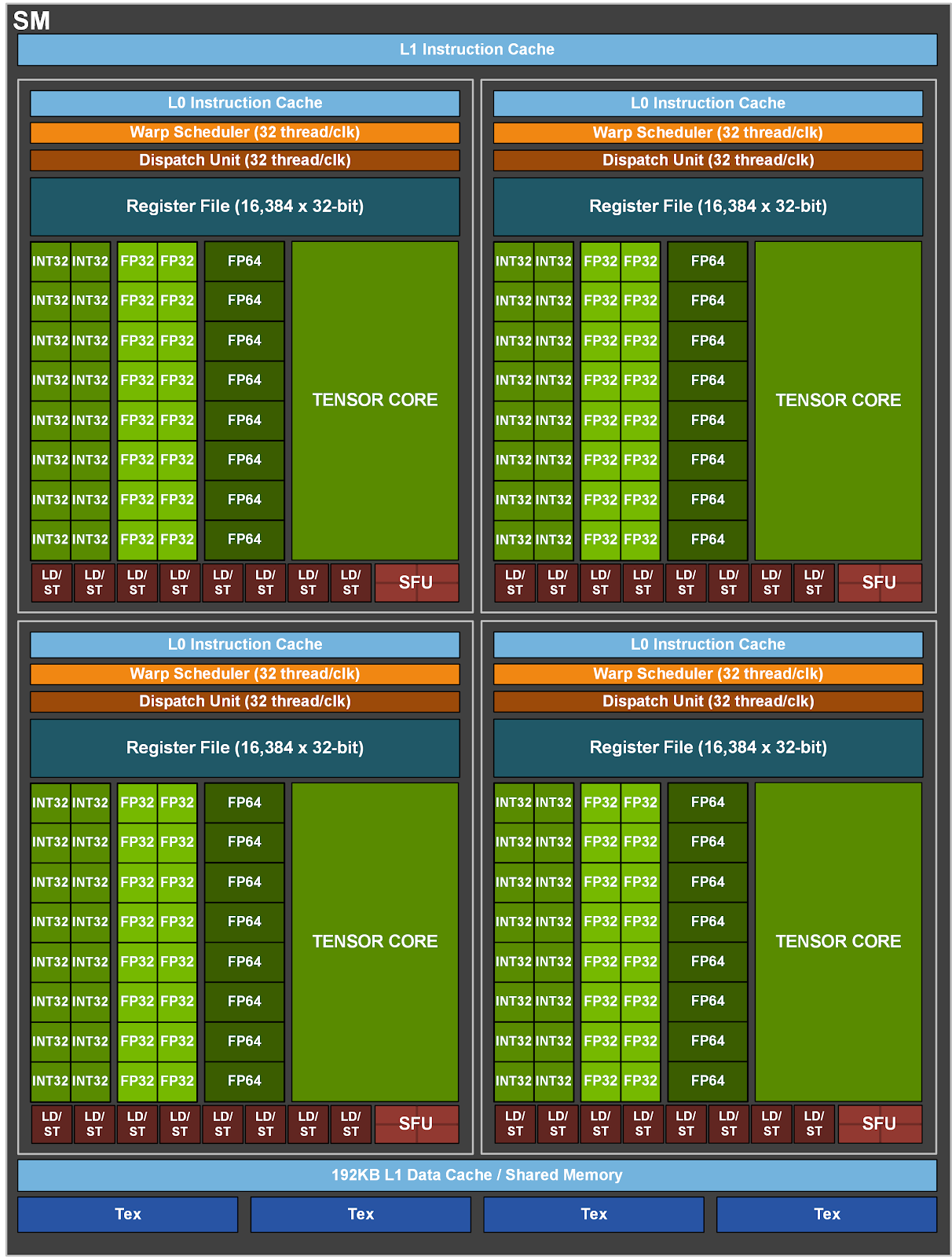
Figure 5. The GA100 streaming multiprocessor (SM).
Figure 6 compares V100 and A100 FP16 Tensor Core operations, and also compares V100 FP32, FP64, and INT8 standard operations to respective A100 TF32, FP64, and INT8 Tensor Core operations. Throughputs are aggregate per GPU, with A100 using sparse Tensor Core operations for FP16, TF32, and INT8. The upper left diagram shows two V100 FP16 Tensor Cores, because a V100 SM has two Tensor Cores per SM partition while an A100 SM one.
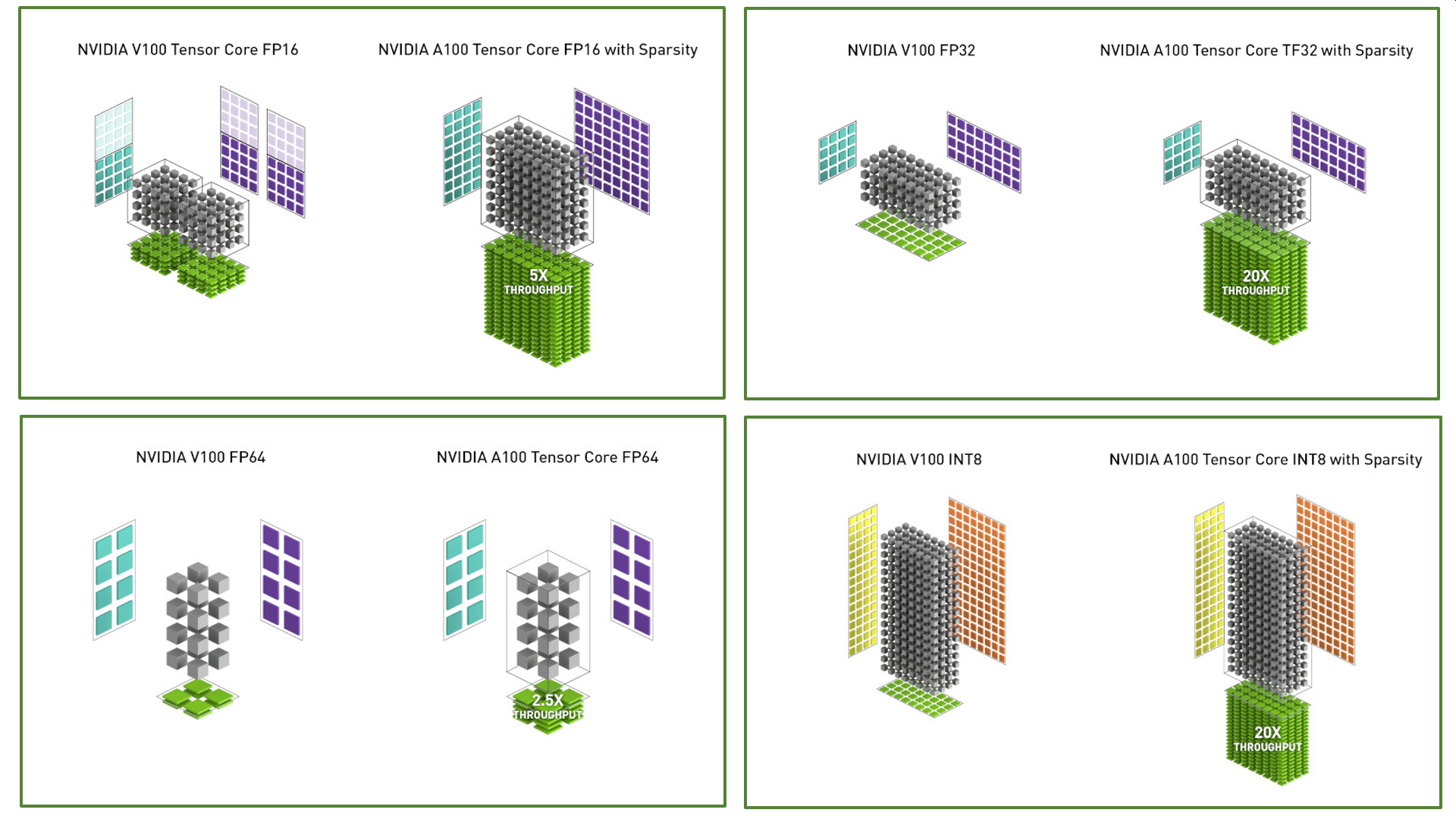
Figure 6. A100 Tensor Core operations compared to V100 Tensor Core and standard operations for different data types.
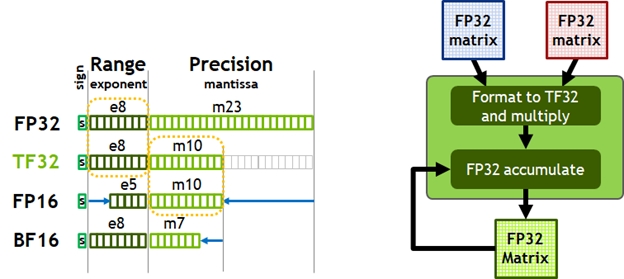
Figure 7. TensorFloat-32 (TF32) provides the range of FP32 with the precision of FP16 (left). A100 accelerates tensor math with TF32 while supporting FP32 input and output data (right), enabling easy integration into DL and HPC programs and automatic acceleration of DL frameworks.
Today, the default math for AI training is FP32, without tensor core acceleration. The NVIDIA Ampere architecture introduces new support for TF32, enabling AI training to use tensor cores by default with no effort on the user’s part. Non-tensor operations continue to use the FP32 datapath, while TF32 tensor cores read FP32 data and use the same range as FP32 with reduced internal precision, before producing a standard IEEE FP32 output. TF32 includes an 8-bit exponent (same as FP32), 10-bit mantissa (same precision as FP16), and 1 sign-bit.
As with Volta, Automatic Mixed Precision (AMP) enables you to use mixed precision with FP16 for AI training with just a few lines of code changes. Using AMP, A100 delivers a further 2X faster Tensor Core performance over TF32.
To summarize, the user choices for NVIDIA Ampere architecture math for DL training are as follows:
- By default, TF32 Tensor Cores are used, with no adjustment to user scripts. Up to 8x more throughput compared to FP32 on A100 and up to 10x compared to FP32 on V100.
- FP16 or BF16 mixed-precision training should be used for maximum training speed. Up to 2x more throughput compared to TF32, and up to 16x compared to FP32 on A100 and up to 20x compared to FP32 on V100.
A100 Tensor Cores accelerate HPC
The performance needs of HPC applications are growing rapidly. Many applications from a wide range of scientific and research disciplines rely on double precision (FP64) computations.
To meet the rapidly growing compute needs of HPC computing, the A100 GPU supports Tensor operations that accelerate IEEE-compliant FP64 computations, delivering up to 2.5x the FP64 performance of the NVIDIA Tesla V100 GPU.
The new double precision matrix multiply-add instruction on A100 replaces eight DFMA instructions on V100, reducing instruction fetches, scheduling overhead, register reads, datapath power, and shared memory read bandwidth.
Each SM in A100 computes a total of 64 FP64 FMA operations/clock (or 128 FP64 operations/clock), which is twice the throughput of Tesla V100. The A100 Tensor Core GPU with 108 SMs delivers a peak FP64 throughput of 19.5 TFLOPS, which is 2.5x that of Tesla V100.
With support for these new formats, the A100 Tensor Cores can be used to accelerate HPC workloads, iterative solvers, and various new AI algorithms.
| | V100 | A100 | A100 Sparsity 1 | A100 Speedup | A100 Speedup with Sparsity | | | ------------------------------------- | ----------- | ----------------------- | ---------------- | ------------------------------ | --- | | A100 FP16 vs. V100 FP16 | 31.4 TFLOPS | 78 TFLOPS | N/A | 2.5x | N/A | | A100 FP16 TC vs. V100 FP16 TC | 125 TFLOPS | 312 TFLOPS | 624 TFLOPS | 2.5x | 5x | | A100 BF16 TC vs. V100 FP16 TC | 125 TFLOPS | 312 TFLOPS | 624 TFLOPS | 2.5x | 5x | | A100 FP32 vs. V100 FP32 | 15.7 TFLOPS | 19.5 TFLOPS | N/A | 1.25x | N/A | | A100 TF32 TC vs. V100 FP32 | 15.7 TFLOPS | 156 TFLOPS | 312 TFLOPS | 10x | 20x | | A100 FP64 vs. V100 FP64 | 7.8 TFLOPS | 9.7 TFLOPS | N/A | 1.25x | N/A | | A100 FP64 TC vs. V100 FP64 | 7.8 TFLOPS | 19.5 TFLOPS | N/A | 2.5x | N/A | | A100 INT8 TC vs. V100 INT8 | 62 TOPS | 624 TOPS | 1248 TOPS | 10x | 20x | | A100 INT4 TC | N/A | 1248 TOPS | 2496 TOPS | N/A | N/A | | A100 Binary TC | N/A | 4992 TOPS | N/A | N/A | N/A |
Table 2. A100 speedup over V100 (TC=Tensor Core, GPUs at respective clock speeds).
1) Effective TOPS / TFLOPS using the new Sparsity feature
A100 introduces fine-grained structured sparsity
With the A100 GPU, NVIDIA introduces fine-grained structured sparsity, a novel approach that doubles compute throughput for deep neural networks.
Sparsity is possible in deep learning because the importance of individual weights evolves during the learning process, and by the end of network training, only a subset of weights have acquired a meaningful purpose in determining the learned output. The remaining weights are no longer needed.
Fine grained structured sparsity imposes a constraint on the allowed sparsity pattern, making it more efficient for hardware to do the necessary alignment of input operands. Because deep learning networks are able to adapt weights during the training process based on training feedback, NVIDIA engineers have found in general that the structure constraint does not impact the accuracy of the trained network for inferencing. This enables inferencing acceleration with sparsity.
For training acceleration, sparsity needs to be introduced early in the process to offer a performance benefit, and methodologies for training acceleration without accuracy loss are an active research area.
Sparse matrix definition
Structure is enforced through a new 2:4 sparse matrix definition that allows two non-zero values in every four-entry vector. A100 supports 2:4 structured sparsity on rows, as shown in Figure 9.
Due to the well-defined structure of the matrix, it can be compressed efficiently and reduce memory storage and bandwidth by almost 2x.
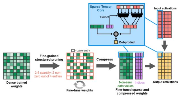
Figure 9. A100 fine-grained structured sparsity prunes trained weights with a 2-out-of-4 non-zero pattern, followed by a simple and universal recipe for fine-tuning the non-zero weights. The weights are compressed for a 2x reduction in data footprint and bandwidth, and the A100 Sparse Tensor Core doubles math throughput by skipping the zeros.
NVIDIA has developed a simple and universal recipe for sparsifying deep neural networks for inference using this 2:4 structured sparsity pattern. The network is first trained using dense weights, then fine-grained structured pruning is applied, and finally the remaining non-zero weights are fine-tuned with additional training steps. This method results in virtually no loss in inferencing accuracy based on evaluation across dozens of networks spanning vision, object detection, segmentation, natural language modeling, and translation.
The A100 Tensor Core GPU includes new Sparse Tensor Core instructions that skip the compute on entries with zero values, resulting in a doubling of the Tensor Core compute throughput. Figure 9 shows how the Tensor Core uses the compression metadata (the non-zero indices) to match the compressed weights with the appropriately selected activations for input to the Tensor Core dot-product computation.
Combined L1 data cache and shared memory
First introduced in NVIDIA Tesla V100, the NVIDIA combined L1 data cache and shared memory subsystem architecture significantly improves performance, while also simplifying programming and reducing the tuning required to attain at or near-peak application performance. Combining data cache and shared memory functionality into a single memory block provides the best overall performance for both types of memory accesses.
The combined capacity of the L1 data cache and shared memory is 192 KB/SM in A100 vs. 128 KB/SM in V100.
Simultaneous execution of FP32 and INT32 operations
Similar to V100 and Turing GPUs, the A100 SM also includes separate FP32 and INT32 cores, allowing simultaneous execution of FP32 and INT32 operations at full throughput, while also increasing instruction issue throughput.
Many applications have inner loops that perform pointer arithmetic (integer memory address calculations) combined with floating-point computations that benefit from simultaneous execution of FP32 and INT32 instructions. Each iteration of a pipelined loop can update addresses (INT32 pointer arithmetic) and load data for the next iteration while simultaneously processing the current iteration in FP32.
A100 HBM2 DRAM subsystem
As HPC, AI, and analytics datasets continue to grow and problems looking for solutions get increasingly complex, more GPU memory capacity and higher memory bandwidth is a necessity.
Tesla P100 was the world’s first GPU architecture to support the high-bandwidth HBM2 memory technology, while Tesla V100 provided a faster, more efficient, and higher capacity HBM2 implementation. A100 raises the bar yet again on HBM2 performance and capacity.
HBM2 memory is composed of memory stacks located on the same physical package as the GPU, providing substantial power and area savings compared to traditional GDDR5/6 memory designs, allowing more GPUs to be installed in systems. For more information about the fundamental details of HBM2 technology, see the NVIDIA Tesla P100: The Most Advanced Datacenter Accelerator Ever Built whitepaper.
The A100 GPU includes 40 GB of fast HBM2 DRAM memory on its SXM4-style circuit board. The memory is organized as five active HBM2 stacks with eight memory dies per stack. With a 1215 MHz (DDR) data rate the A100 HBM2 delivers 1555 GB/sec memory bandwidth, which is more than 1.7x higher than V100 memory bandwidth.
ECC memory resiliency
The A100 HBM2 memory subsystem supports single-error correcting double-error detection (SECDED) error-correcting code (ECC) to protect data. ECC provides higher reliability for compute applications that are sensitive to data corruption. It is especially important in large-scale, cluster computing environments where GPUs process large datasets or run applications for extended periods. Other key memory structures in A100 are also protected by SECDED ECC, including the L2 cache and the L1 caches and register files inside all the SMs.
A100 L2 cache
The A100 GPU includes 40 MB of L2 cache, which is 6.7x larger than V100 L2 cache.The L2 cache is divided into two partitions to enable higher bandwidth and lower latency memory access. Each L2 partition localizes and caches data for memory accesses from SMs in the GPCs directly connected to the partition. This structure enables A100 to deliver a 2.3x L2 bandwidth increase over V100. Hardware cache-coherence maintains the CUDA programming model across the full GPU, and applications automatically leverage the bandwidth and latency benefits of the new L2 cache.
L2 cache is a shared resource for the GPCs and SMs and lies outside of the GPCs. The substantial increase in the A100 L2 cache size significantly improves performance of many HPC and AI workloads because larger portions of datasets and models can now be cached and repeatedly accessed at much higher speed than reading from and writing to HBM2 memory. Some workloads that are limited by DRAM bandwidth will benefit from the larger L2 cache, such as deep neural networks using small batch sizes.
To optimize capacity utilization, the NVIDIA Ampere architecture provides L2 cache residency controls for you to manage data to keep or evict from the cache. You can set aside a portion of L2 cache for persistent data accesses.
For example, for DL inferencing workloads, ping-pong buffers can be persistently cached in the L2 for faster data access, while also avoiding writebacks to DRAM. For producer-consumer chains, such as those found in DL training, L2 cache controls can optimize caching across the write-to-read data dependencies. In LSTM networks, recurrent weights can be preferentially cached and reused in L2.
The NVIDIA Ampere architecture adds Compute Data Compression to accelerate unstructured sparsity and other compressible data patterns. Compression in L2 provides up to 4x improvement to DRAM read/write bandwidth, up to 4x improvement in L2 read bandwidth, and up to 2x improvement in L2 capacity.
| Data Center GPU | NVIDIA Tesla P100 | NVIDIA Tesla V100 | NVIDIA A100 |
|---|---|---|---|
| GPU Codename | GP100 | GV100 | GA100 |
| GPU Architecture | NVIDIA Pascal | NVIDIA Volta | NVIDIA Ampere |
| GPU Board Form Factor | SXM | SXM2 | SXM4 |
| SMs | 56 | 80 | 108 |
| TPCs | 28 | 40 | 54 |
| FP32 Cores / SM | 64 | 64 | 64 |
| FP32 Cores / GPU | 3584 | 5120 | 6912 |
| FP64 Cores / SM | 32 | 32 | 32 |
| FP64 Cores / GPU | 1792 | 2560 | 3456 |
| INT32 Cores / SM | NA | 64 | 64 |
| INT32 Cores / GPU | NA | 5120 | 6912 |
| Tensor Cores / SM | NA | 8 | 42 |
| Tensor Cores / GPU | NA | 640 | 432 |
| GPU Boost Clock | 1480 MHz | 1530 MHz | 1410 MHz |
| Peak FP16 Tensor TFLOPS with FP16 Accumulate1 | NA | 125 | 312/6243 |
| Peak FP16 Tensor TFLOPS with FP32 Accumulate1 | NA | 125 | 312/6243 |
| Peak BF16 Tensor TFLOPS with FP32 Accumulate1 | NA | NA | 312/6243 |
| Peak TF32 Tensor TFLOPS1 | NA | NA | 156/3123 |
| Peak FP64 Tensor TFLOPS1 | NA | NA | 19.5 |
| Peak INT8 Tensor TOPS1 | NA | NA | 624/12483 |
| Peak INT4 Tensor TOPS1 | NA | NA | 1248/24963 |
| Peak FP16 TFLOPS1 | 21.2 | 31.4 | 78 |
| Peak BF16 TFLOPS1 | NA | NA | 39 |
| Peak FP32 TFLOPS1 | 10.6 | 15.7 | 19.5 |
| Peak FP64 TFLOPS1 | 5.3 | 7.8 | 9.7 |
| Peak INT32 TOPS1,4 | NA | 15.7 | 19.5 |
| Texture Units | 224 | 320 | 432 |
| Memory Interface | 4096-bit HBM2 | 4096-bit HBM2 | 5120-bit HBM2 |
| Memory Size | 16 GB | 32 GB / 16 GB | 40 GB |
| Memory Data Rate | 703 MHz DDR | 877.5 MHz DDR | 1215 MHz DDR |
| Memory Bandwidth | 720 GB/sec | 900 GB/sec | 1555 GB/sec |
| L2 Cache Size | 4096 KB | 6144 KB | 40960 KB |
| Shared Memory Size / SM | 64 KB | Configurable up to 96 KB | Configurable up to 164 KB |
| Register File Size / SM | 256 KB | 256 KB | 256 KB |
| Register File Size / GPU | 14336 KB | 20480 KB | 27648 KB |
| TDP | 300 Watts | 300 Watts | 400 Watts |
| Transistors | 15.3 billion | 21.1 billion | 54.2 billion |
| GPU Die Size | 610 mm² | 815 mm² | 826 mm2 |
| TSMC Manufacturing Process | 16 nm FinFET+ | 12 nm FFN | 7 nm N7 |
Table 3. Comparison of NVIDIA data center GPUs.
- Peak rates are based on the GPU boost clock.
- Four Tensor Cores in an A100 SM have 2x the raw FMA computational power of eight Tensor Cores in a GV100 SM.
- Effective TOPS / TFLOPS using the new Sparsity feature.
- TOPS = IMAD-based integer math
Note: Because the A100 Tensor Core GPU is designed to be installed in high-performance servers and data center racks to power AI and HPC compute workloads, it does not include display connectors, NVIDIA RT Cores for ray tracing acceleration, or an NVENC encoder.
Compute capability
The A100 GPU supports the new compute capability 8.0. Table 4 compares the parameters of different compute capabilities for NVIDIA GPU architectures.
| Data center GPU | NVIDIA Tesla P100 | NVIDIA Tesla V100 | NVIDIA A100 |
|---|---|---|---|
| GPU Codename | GP100 | GV100 | GA100 |
| GPU Architecture | NVIDIA Pascal | NVIDIA Volta | NVIDIA Ampere |
| Compute Capability | 6.0 | 7.0 | 8.0 |
| Threads / Warp | 32 | 32 | 32 |
| Max Warps / SM | 64 | 64 | 64 |
| Max Threads / SM | 2048 | 2048 | 2048 |
| Max Thread Blocks / SM | 32 | 32 | 32 |
| Max 32-bit Registers / SM | 65536 | 65536 | 65536 |
| Max Registers / Block | 65536 | 65536 | 65536 |
| Max Registers / Thread | 255 | 255 | 255 |
| Max Thread Block Size | 1024 | 1024 | 1024 |
| FP32 Cores / SM | 64 | 64 | 64 |
| Ratio of SM Registers to FP32 Cores | 1024 | 1024 | 1024 |
| Shared Memory Size / SM | 64 KB | Configurable up to 96 KB | Configurable up to 164 KB |
Table 4. Compute Capability: GP100 vs. GV100 vs. GA100.
MIG architecture
While many data center workloads continue to scale, both in size and complexity, some acceleration tasks aren’t as demanding, such as early-stage development or inference on simple models at low batch sizes. Data center managers aim to keep resource utilization high, so an ideal data center accelerator doesn’t just go big—it also efficiently accelerates many smaller workloads.
The new MIG feature can partition each A100 into as many as seven GPU Instances for optimal utilization, effectively expanding access to every user and application.
Figure 10 shows how Volta MPS allowed multiple applications to simultaneously execute on separate GPU execution resources (SMs). However, because memory system resources were shared across all the applications, one application could interfere with the others if it had high demands for DRAM bandwidth or its requests oversubscribed the L2 cache.
The A100 GPU new MIG capability shown in Figure 11 can divide a single GPU into multiple GPU partitions called GPU instances. Each instance’s SMs have separate and isolated paths through the entire memory system – the on-chip crossbar ports, L2 cache banks, memory controllers and DRAM address busses are all assigned uniquely to an individual instance. This ensures that an individual user’s workload can run with predictable throughput and latency, with the same L2 cache allocation and DRAM bandwidth, even if other tasks are thrashing their own caches or saturating their DRAM interfaces.
Using this capability, MIG can partition available GPU compute resources to provide a defined quality of service (QoS) with fault isolation for different clients (such as VMs, containers, processes, and so on). It enables multiple GPU Instances to run in parallel on a single, physical A100 GPU. MIG also keeps the CUDA programming model unchanged to minimize programming effort.
CSPs can use MIG to raise utilization rates on their GPU servers, delivering up to 7x more GPU Instances at no additional cost. MIG supports the necessary QoS and isolation guarantees needed by CSPs to ensure that one client (VM, container, process) cannot impact the work or scheduling from another client.
CSPs often partition their hardware based on customer usage patterns. Effective partitioning only works if hardware resources are providing consistent bandwidth, proper isolation, and good performance during runtime.
With NVIDIA Ampere architecture-based GPU, you can see and schedule jobs on their new virtual GPU instances as if they were physical GPUs. MIG works with Linux operating systems and their hypervisors. Users can run containers with MIG using runtimes such as Docker Engine, with support for container orchestration using Kubernetes coming soon.
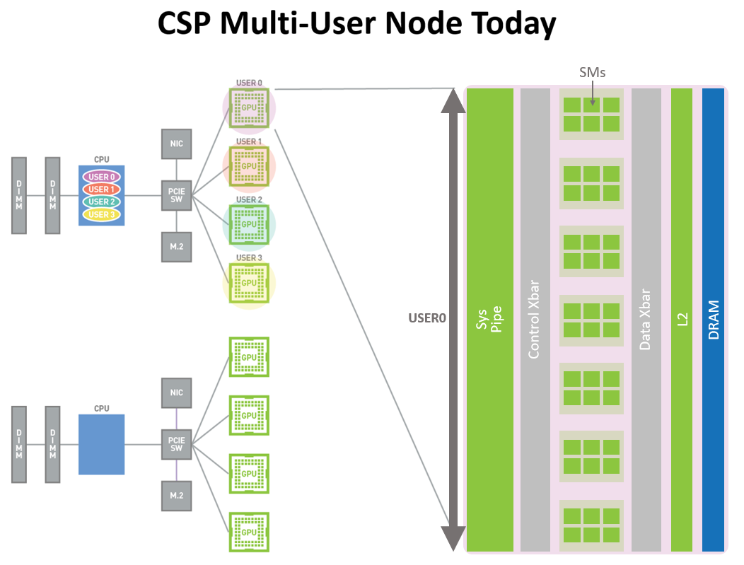
Figure 10. CSP Multi-user node today (pre-A100). Accelerated GPU instances are available for usage only at full physical GPU granularity for users in different organizations, even if the user applications don’t require a full GPU.
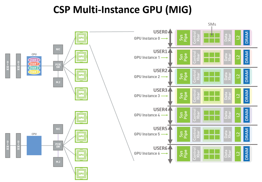
Figure 11. CSP multi-user with MIG diagram. Multiple independent users from the same or different organizations can be assigned their own dedicated, protected, and isolated GPU Instance within a single physical GPU.
Error and fault detection, isolation, and containment
It is critically important to improve GPU uptime and availability by detecting, containing, and often correcting errors and faults, rather than forcing GPU resets. This is especially important in large, multi-GPU clusters and single-GPU, multi-tenant environments such as MIG configurations.
The NVIDIA Ampere architecture A100 GPU includes new technology to improve error/fault attribution (attribute the applications that are causing errors), isolation (isolate faulty applications so that they do not affect other applications running on the same GPU or in a GPU cluster), and containment (ensure that errors in one application do not leak and affect other applications). These fault-handling technologies are particularly important for MIG environments to ensure proper isolation and security between clients sharing the single GPU.
NVLink-connected GPUs now have more robust error-detection and recovery features. Page faults at the remote GPU are sent back to the source GPU through NVLink. Remote access fault communication is a critical resiliency feature for large GPU computing clusters to help ensure that faults in one process or VM do not bring down other processes or VMs.
The A100 GPU includes several other new and improved hardware features that enhance application performance. For more information, see the NVIDIA A100 Tensor Core GPU Architecturewhitepaper.
CUDA 11 advances for NVIDIA Ampere architecture GPUs
Thousands of GPU-accelerated applications are built on the NVIDIA CUDA parallel computing platform. The flexibility and programmability of CUDA have made it the platform of choice for researching and deploying new DL and parallel computing algorithms.
NVIDIA Ampere architecture GPUs are designed to improve GPU programmability and performance, while also reducing software complexity. NVIDIA Ampere architecture GPUs and the CUDA programming model advances accelerate program execution and lower the latency and overhead of many operations.
New CUDA 11 features provide programming and API support for third-generation Tensor Cores, Sparsity, CUDA graphs, multi-instance GPUs, L2 cache residency controls, and several other new capabilities of the NVIDIA Ampere architecture.
For more information about the new CUDA features, see the NVIDIA A100 Tensor Core GPU Architecture whitepaper. For more information about the new DGX A100 system, see Defining AI Innovation with NVIDIA DGX A100. For more information about the Developer Zone, see NVIDIA Developer, and for more information about CUDA, see the new CUDA Programming Guide.
Conclusion
The NVIDIA mission is to accelerate the work of the da Vincis and Einsteins of our time. Scientists, researchers, and engineers are focused on solving some of the world’s most important scientific, industrial, and big data challenges using high performance computing (HPC) and AI.
The NVIDIA A100 Tensor Core GPU delivers the next giant leap in our accelerated data center platform, providing unmatched acceleration at every scale and enabling these innovators to do their life’s work in their lifetime. A100 powers numerous application areas including HPC, genomics, 5G, rendering, deep learning, Data analytics, data science, and robotics.
Advancing the most important HPC and AI applications today—personalized medicine, conversational AI, and deep recommender systems—requires researchers to go big. A100 powers the NVIDIA data center platform that includes Mellanox HDR InfiniBand, NVSwitch, NVIDIA HGX A100, and the Magnum IO SDK for scaling up. This integrated team of technologies efficiently scales to tens of thousands of GPUs to train the most complex AI networks at unprecedented speed.
The new MIG feature of the A100 GPU can partition each A100 into as many as seven GPU accelerators for optimal utilization, effectively improving GPU resource utilization and GPU access to more users and GPU-accelerated applications. With the A100 versatility, infrastructure managers can maximize the utility of every GPU in their data center to meet different-sized performance needs, from the smallest job to the biggest multi-node workload.
Acknowledgments
We would like to thank Vishal Mehta, Manindra Parhy, Eric Viscito, Kyrylo Perelygin, Asit Mishra, Manas Mandal, Luke Durant, Jeff Pool, Jay Duluk, Piotr Jaroszynski, Brandon Bell, Jonah Alben, and many other NVIDIA architects and engineers who contributed to this post.