Single-shot readout of an electron spin in silicon (original) (raw)
- Letter
- Published: 26 September 2010
- Jarryd J. Pla1,
- Floris A. Zwanenburg1,
- Kok W. Chan1,
- Kuan Y. Tan1,
- Hans Huebl1 nAff5,
- Mikko Möttönen1,3,4,
- Christopher D. Nugroho1 nAff5,
- Changyi Yang2,
- Jessica A. van Donkelaar2,
- Andrew D. C. Alves2,
- David N. Jamieson2,
- Christopher C. Escott1,
- Lloyd C. L. Hollenberg2,
- Robert G. Clark1 nAff5 &
- …
- Andrew S. Dzurak1
Nature volume 467, pages 687–691 (2010)Cite this article
- 24k Accesses
- 712 Citations
- 77 Altmetric
- Metrics details
Subjects
Abstract
The size of silicon transistors used in microelectronic devices is shrinking to the level at which quantum effects become important1. Although this presents a significant challenge for the further scaling of microprocessors, it provides the potential for radical innovations in the form of spin-based quantum computers2,3,4 and spintronic devices5. An electron spin in silicon can represent a well-isolated quantum bit with long coherence times6 because of the weak spin–orbit coupling7 and the possibility of eliminating nuclear spins from the bulk crystal8. However, the control of single electrons in silicon has proved challenging, and so far the observation and manipulation of a single spin has been impossible. Here we report the demonstration of single-shot, time-resolved readout of an electron spin in silicon. This has been performed in a device consisting of implanted phosphorus donors9 coupled to a metal-oxide-semiconductor single-electron transistor10,11—compatible with current microelectronic technology. We observed a spin lifetime of ∼6 seconds at a magnetic field of 1.5 tesla, and achieved a spin readout fidelity better than 90 per cent. High-fidelity single-shot spin readout in silicon opens the way to the development of a new generation of quantum computing and spintronic devices, built using the most important material in the semiconductor industry.
This is a preview of subscription content, access via your institution
Access options
Subscribe to this journal
Receive 51 print issues and online access
$199.00 per year
only $3.90 per issue
Buy this article
- Purchase on SpringerLink
- Instant access to the full article PDF.
USD 39.95
Prices may be subject to local taxes which are calculated during checkout
Additional access options:
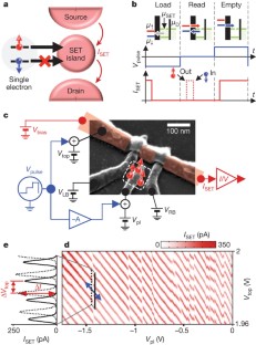
Figure 1: Spin readout device configuration and charge transitions.
The alternative text for this image may have been generated using AI.
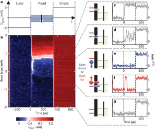
Figure 2: Single-shot spin readout and calibration of the ‘read’ level.
The alternative text for this image may have been generated using AI.
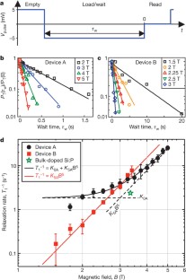
Figure 3: Spin relaxation rate.
The alternative text for this image may have been generated using AI.
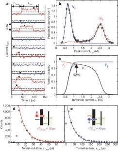
Figure 4: Readout fidelity and visibility.
The alternative text for this image may have been generated using AI.
References
- Levi, A. J. F. Towards quantum engineering. Proc. IEEE 96, 335–342 (2008)
Article Google Scholar - Loss, D. & DiVincenzo, D. P. Quantum computation with quantum dots. Phys. Rev. A 57, 120–126 (1998)
Article ADS CAS Google Scholar - Kane, B. E. A silicon-based nuclear spin quantum computer. Nature 393, 133–137 (1998)
Article ADS CAS Google Scholar - Hollenberg, L. C. L., Greentree, A. D., Fowler, A. G. & Wellard, C. J. Two-dimensional architectures for donor-based quantum computing. Phys. Rev. B 74, 045311 (2006)
Article ADS Google Scholar - Žutić, I., Fabian, J. & Das Sarma, S. Spintronics: fundamentals and applications. Rev. Mod. Phys. 76, 323–410 (2004)
Article ADS Google Scholar - Tyryshkin, A. M., Lyon, S. A., Astashkin, A. V. & Raitsimring, A. M. Electron spin relaxation times of phosphorus donors in silicon. Phys. Rev. B 68, 193207 (2003)
Article ADS Google Scholar - Feher, G. & Gere, E. A. Electron spin resonance experiments on donors in silicon. II. Electron spin relaxation effects. Phys. Rev. 114, 1245–1256 (1959)
Article ADS CAS Google Scholar - Ager, J. W. et al. High-purity, isotopically enriched bulk silicon. J. Electrochem. Soc. 152, G448–G451 (2005)
Article CAS Google Scholar - Jamieson, D. N. et al. Controlled shallow single-ion implantation in silicon using an active substrate for sub-20-keV ions. Appl. Phys. Lett. 86, 202101 (2005)
Article ADS Google Scholar - Angus, S. J., Ferguson, A. J., Dzurak, A. S. & Clark, R. G. Gate-defined quantum dots in intrinsic silicon. Nano Lett. 7, 2051–2055 (2007)
Article ADS CAS Google Scholar - Morello, A. et al. Architecture for high-sensitivity single-shot readout and control of the electron spin of individual donors in silicon. Phys. Rev. B 80, 081307(R) (2009)
Article ADS Google Scholar - Ladd, T. D. et al. Quantum computers. Nature 464, 45–53 (2010)
Article ADS CAS Google Scholar - Elzerman, J. M. et al. Single-shot read-out of an individual electron spin in a quantum dot. Nature 430, 431–435 (2004)
Article ADS CAS Google Scholar - Hanson, R. et al. Single-shot readout of electron spin states in a quantum dot using spin-dependent tunnel rates. Phys. Rev. Lett. 94, 196802 (2005)
Article ADS CAS Google Scholar - Barthel, C., Reilly, D. J., Marcus, C. M., Hanson, M. P. & Gossard, A. C. Rapid single-shot measurement of a singlet-triplet qubit. Phys. Rev. Lett. 103, 160503 (2009)
Article ADS CAS Google Scholar - Devoret, M. H. & Schoelkopf, R. J. Amplifying quantum signals with the single-electron transistor. Nature 406, 1039–1046 (2000)
Article CAS Google Scholar - Goswami, S., et al. Controllable valley splitting in silicon quantum devices.Nature Phys. 3, 41–45 (2007); published online 10 December 2006.
Article ADS Google Scholar - Morton, J. J. L. et al. Solid-state quantum memory using the 31P nuclear spin. Nature 455, 1085–1088 (2008)
Article ADS CAS Google Scholar - Hofmann, F. et al. Single electron switching in a parallel quantum dot. Phys. Rev. B 51, 13872–13875 (1995)
Article ADS CAS Google Scholar - Huebl, H. et al. Electron tunnel rates in a donor-silicon single electron transistor hybrid. Phys. Rev. B 81, 235318 (2010)
Article ADS Google Scholar - Tan, K. Y. et al. Transport spectroscopy of single phosphorus donors in a silicon nanoscale transistor. Nano Lett. 10, 11–15 (2010)
Article ADS CAS Google Scholar - DiVincenzo, D. P. The physical implementation of quantum computation. Fortschr. Phys. 48, 771–783 (2000)
Article Google Scholar - Hanson, R., Kouwenhoven, L. P., Petta, J. R., Tarucha, S. & Vandersypen, L. K. Spins in few-electron quantum dots. Rev. Mod. Phys. 79, 1217–1265 (2007)
Article ADS CAS Google Scholar - Hasegawa, H. Spin-lattice relaxation of shallow donor states in Ge and Si through a direct phonon process. Phys. Rev. 118, 1523–1534 (1960)
Article ADS CAS Google Scholar - Hayes, R. R. et al. Lifetime measurements (T 1) of electron spins in Si/SiGe quantum dots. Preprint at 〈http://arxiv.org/abs/0908.0173〉 (2009)
- Xiao, M., House, M. G. & Jiang, H. W. Measurement of the spin relaxation time of single electrons in a silicon metal-oxide-semiconductor-based quantum dot. Phys. Rev. Lett. 104, 096801 (2010)
Article ADS CAS Google Scholar - de Sousa, R. Dangling-bond spin relaxation and magnetic 1/f noise from the amorphous-semiconductor/oxide interface: theory. Phys. Rev. B 76, 245306 (2007)
Article ADS Google Scholar - Shankar, S., Tyryshkin, A. M., He, J. & Lyon, S. A. Spin relaxation and coherence times for electrons at the Si/SiO2 interface. Preprint at 〈http://arxiv.org/abs/0912.3037〉 (2009)
- Calderón, M. J., Saraiva, A., Koiller, B. & Das Sarma, S. Quantum control and manipulation of donor electrons in Si-based quantum computing. Appl. Phys. Lett. 105, 122410 (2009)
Google Scholar - Xiao, M., Martin, I., Yablonovitch, E. & Jiang, H. W. Electrical detection of the spin resonance of a single electron in a silicon field-effect transistor. Nature 430, 435–439 (2004)
Article ADS CAS Google Scholar
Acknowledgements
We thank D. D. Awschalom, C. Tahan, J. J. L. Morton and G. Prawiroatmodjo for comments and suggestions, W. H. Lim for assistance with device fabrication, and R. P. Starrett, D. Barber, A. Cimmino and R. Szymanski for technical assistance. We acknowledge support from the Australian Research Council, the Australian Government, the US National Security Agency and the US Army Research Office under contract number W911NF-08-1-0527. M.M. acknowledges support from the Academy of Finland and the Emil Aaltonen foundation.
Author information
Author notes
- Hans Huebl, Christopher D. Nugroho & Robert G. Clark
Present address: Present addresses: Walther-Meissner-Institut, Bayerische Akademie der Wissenschaften, 85748 Garching, Germany (H.H.); Department of Physics, University of Illinois at Urbana-Champaign, Urbana, Illinois 61801, USA (C.D.N.); Department of Defence, Canberra, Australian Capital Territory 2600, Australia (R.G.C.).,
Authors and Affiliations
- Australian Research Council Centre of Excellence for Quantum Computer Technology, School of Electrical Engineering and Telecommunications, University of New South Wales, Sydney, New South Wales 2052, Australia ,
Andrea Morello, Jarryd J. Pla, Floris A. Zwanenburg, Kok W. Chan, Kuan Y. Tan, Hans Huebl, Mikko Möttönen, Christopher D. Nugroho, Christopher C. Escott, Robert G. Clark & Andrew S. Dzurak - Australian Research Council Centre of Excellence for Quantum Computer Technology, School of Physics, University of Melbourne, Melbourne, Victoria 3010, Australia ,
Changyi Yang, Jessica A. van Donkelaar, Andrew D. C. Alves, David N. Jamieson & Lloyd C. L. Hollenberg - Department of Applied Physics/COMP, Aalto University, PO Box 15100, 00076 Aalto, Finland,
Mikko Möttönen - Low Temperature Laboratory, Aalto University, PO Box 13500, 00076 Aalto, Finland ,
Mikko Möttönen
Authors
- Andrea Morello
- Jarryd J. Pla
- Floris A. Zwanenburg
- Kok W. Chan
- Kuan Y. Tan
- Hans Huebl
- Mikko Möttönen
- Christopher D. Nugroho
- Changyi Yang
- Jessica A. van Donkelaar
- Andrew D. C. Alves
- David N. Jamieson
- Christopher C. Escott
- Lloyd C. L. Hollenberg
- Robert G. Clark
- Andrew S. Dzurak
Contributions
A.M., H.H., C.D.N., D.N.J., C.C.E., L.C.L.H., R.G.C. (while at UNSW) and A.S.D. conceived and designed the experiment, K.W.C. and K.Y.T. fabricated the devices, C.Y., J.A.v.D., A.D.C.A. and D.N.J. implanted the P donors, A.M., J.J.P. and F.A.Z. performed and analysed the measurements, A.M., M.M. and J.J.P. analysed the readout fidelity. A.M. wrote the manuscript with input from all coauthors
Corresponding author
Correspondence toAndrea Morello.
Ethics declarations
Competing interests
The authors declare no competing financial interests.
Supplementary information
Supplementary Information (download PDF )
The file contains Supplementary Information on Deterministic loading of the spin ground state and measurement of the Zeeman energy splitting, measurement methods and analysis of the spin relaxation rate and readout fidelity and calculation of the distribution of peak currents. The file also contains Supplementary Figures 1-4 with legends and additional references. (PDF 509 kb)
PowerPoint slides
Rights and permissions
About this article
Cite this article
Morello, A., Pla, J., Zwanenburg, F. et al. Single-shot readout of an electron spin in silicon.Nature 467, 687–691 (2010). https://doi.org/10.1038/nature09392
- Received: 28 April 2010
- Accepted: 02 August 2010
- Published: 26 September 2010
- Issue date: 07 October 2010
- DOI: https://doi.org/10.1038/nature09392
This article is cited by
Editorial Summary
Taking aim at silicon
Silicon transistors in microelectronics are shrinking to close to the size at which quantum effects begin to have an impact on device performance. As silicon looks certain to remain the semiconductor material of choice for a while yet, such effects may be turned into an advantage by designing silicon devices that can process quantum information. One approach is to make use of electron spins generated by phosphorus dopant atoms buried in silicon, as they are known to represent well-isolated quantum bits (qubits) with long coherence times. It has not been possible to control single electrons in silicon with the precision for qubits, but now Andrea Morello and colleagues report single-shot, time-resolved readout of electron spins in silicon. This is achieved by placing the phosphorus donor atoms near a charge-sensing device called a single-electron transistor, which is fully compatible with current microelectronic technology. The demonstrated high-fidelity single-shot spin readout opens a path to the development of a new generation of quantum computing and spintronic devices in silicon.