Gate-tuning of graphene plasmons revealed by infrared nano-imaging (original) (raw)
- Letter
- Published: 20 June 2012
- A. S. Rodin1,
- G. O. Andreev1,
- W. Bao2,3,
- A. S. McLeod1,
- M. Wagner1,
- L. M. Zhang4,
- Z. Zhao2,
- M. Thiemens5,
- G. Dominguez6,
- M. M. Fogler1,
- A. H. Castro Neto7,
- C. N. Lau2,
- F. Keilmann8 &
- …
- D. N. Basov1
Nature volume 487, pages 82–85 (2012) Cite this article
- 40k Accesses
- 2102 Citations
- 55 Altmetric
- Metrics details
Subjects
Abstract
Surface plasmons are collective oscillations of electrons in metals or semiconductors that enable confinement and control of electromagnetic energy at subwavelength scales1,2,3,4,5. Rapid progress in plasmonics has largely relied on advances in device nano-fabrication5,6,7, whereas less attention has been paid to the tunable properties of plasmonic media. One such medium—graphene—is amenable to convenient tuning of its electronic and optical properties by varying the applied voltage8,9,10,11. Here, using infrared nano-imaging, we show that common graphene/SiO2/Si back-gated structures support propagating surface plasmons. The wavelength of graphene plasmons is of the order of 200 nanometres at technologically relevant infrared frequencies, and they can propagate several times this distance. We have succeeded in altering both the amplitude and the wavelength of these plasmons by varying the gate voltage. Using plasmon interferometry, we investigated losses in graphene by exploring real-space profiles of plasmon standing waves formed between the tip of our nano-probe and the edges of the samples. Plasmon dissipation quantified through this analysis is linked to the exotic electrodynamics of graphene10. Standard plasmonic figures of merit of our tunable graphene devices surpass those of common metal-based structures.
This is a preview of subscription content, access via your institution
Access options
Subscribe to this journal
Receive 52 print issues and online access
$199.00 per year
only $3.83 per issue
Buy this article
- Purchase on SpringerLink
- Instant access to the full article PDF.
USD 39.95
Prices may be subject to local taxes which are calculated during checkout
Additional access options:
Figure 1: Infrared nano-imaging experiment and results.
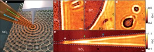
The alternative text for this image may have been generated using AI.
Figure 2: Spatial variation of the electric field and near-field amplitude at the graphene edge.
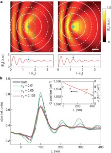
The alternative text for this image may have been generated using AI.
Figure 3: Electrostatically tunable plasmons in back-gated graphene.
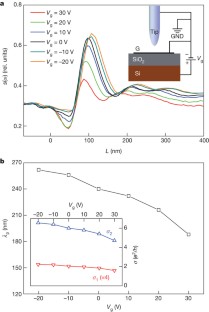
The alternative text for this image may have been generated using AI.
References
- Atwater, H. A. The promise of plasmonics. Sci. Am. 296, 56–62 (2007)
Article CAS Google Scholar - West, P. R. et al. Searching for better plasmonic materials. Laser Photon. Rev. 4, 795–808 (2010)
Article CAS ADS Google Scholar - Stockman, M. I. Nanoplasmonics: the physics behind the applications. Phys. Today 64, 39–44 (2011)
Article Google Scholar - Maier, S. A. Plasmonics: Fundamentals and Applications Ch. 4 (Springer, 2007)
Book Google Scholar - Schuller, J. A. et al. Plasmonics for extreme light concentration and manipulation. Nature Mater. 9, 193–204 (2010)
Article CAS ADS Google Scholar - Nagpal, P., Lindquist, N. C., Oh, S.-H. & Norris, D. J. Ultrasmooth patterned metals for plasmonics and metamaterials. Science 325, 594–597 (2009)
Article CAS ADS Google Scholar - Lal, S., Link, S. & Halas, N. J. Nano-optics from sensing to waveguiding. Nature Photon. 1, 641–648 (2007)
Article CAS ADS Google Scholar - Castro Neto, A. H., Guinea, F., Peres, N. M. R., Novoselov, K. S. & Geim, A. K. The electronic properties of graphene. Rev. Mod. Phys. 81, 109–162 (2009)
Article CAS ADS Google Scholar - Wang, F. et al. Gate-variable optical transitions in graphene. Science 320, 206–209 (2008)
Article CAS ADS Google Scholar - Li, Z. Q. et al. Dirac charge dynamics in graphene by infrared spectroscopy. Nature Phys. 4, 532–535 (2008)
Article CAS ADS Google Scholar - Vakil, A. & Engheta, N. Transformation optics using graphene. Science 332, 1291–1294 (2011)
Article CAS ADS Google Scholar - Jablan, M., Buljan, H. & Soljacic, M. Plasmonics in graphene at infrared frequencies. Phys. Rev. B 80, 245435 (2009)
Article ADS Google Scholar - Fei, Z. et al. Infrared nanoscopy of Dirac plasmons at the graphene-SiO2 interface. Nano Lett. 11, 4701–4705 (2011)
Article CAS ADS Google Scholar - Ju, L. et al. Graphene plasmonics for tunable terahertz metamaterials. Nature Nanotechnol. 6, 630–634 (2011)
Article CAS ADS Google Scholar - Huber, A., Ocelic, N., Kazantsev, D. & Hillenbrand, R. Near-field imaging of mid-infrared surface phonon polariton propagation. Appl. Phys. Lett. 87, 081103 (2005)
Article ADS Google Scholar - Dallapiccola, R., Dubois, C., Gopinath, A., Stellacci, F. & Dal Negro, L. Near-field excitation and near-field detection of propagating surface plasmon polaritons on Au waveguide structures. Appl. Phys. Lett. 94, 243118 (2009)
Article ADS Google Scholar - Casiraghi, C. et al. Raman spectroscopy of graphene edges. Nano Lett. 9, 1433–1441 (2009)
Article CAS ADS Google Scholar - Caridad, J. M. et al. Effects of particle contamination and substrate interaction on the Raman response of unintentionally doped graphene. J. Appl. Phys. 108, 084321 (2010)
Article ADS Google Scholar - Hwang, E. H. & Das Sarma, S. Dielectric function, screening, and plasmons in two-dimensional graphene. Phys. Rev. B 75, 205418 (2007)
Article ADS Google Scholar - Ando, T., Zheng, Y. & Suzuura, H. Dynamical conductivity and zero-mode anomaly in honeycomb lattices. J. Phys. Soc. Jpn 71, 1318–1324 (2002)
Article CAS ADS Google Scholar - Peres, N. M. R., Guinea, F. & Castro Neto, A. H. Electronic properties of disordered two-dimensional carbon. Phys. Rev. B 73, 125411 (2006)
Article ADS Google Scholar - Gusynin, V. P. & Sharapov, S. G. Transport of Dirac quasiparticles in graphene: Hall and optical conductivities. Phys. Rev. B 73, 245411 (2006)
Article ADS Google Scholar - Grushin, A. G., Valenzuela, B. & Vozmediano, M. A. H. Effect of Coulomb interactions on the optical properties of doped graphene. Phys. Rev. B 80, 155417 (2009)
Article ADS Google Scholar - Peres, N. M. R., Ribeiro, R. M. & Castro-Neto, A. H. Excitonic effects in the optical conductivity of gated graphene. Phys. Rev. Lett. 105, 055501 (2010)
Article CAS ADS Google Scholar - Hwang, J., Leblanc, J. P. F. & Carbotte, J. P. Optical self-energy in graphene due to correlations. J. Phys. Condens. Matter 24, 245601 (2012)
Article CAS ADS Google Scholar - Rana, F. Graphene terahertz plasmon oscillators. IEEE Trans. Nanotechol. 7, 91–99 (2008)
Article ADS Google Scholar - Chen, J. et al. Optical nano-imaging of gate-tunable graphene plasmons. Nature http://dx.doi.org/10.1038/nature11254 (this issue).
- Novotny, L. & Hecht, B. Principles of Nano-Optics (Cambridge Univ. Press, 2006)
Book Google Scholar - Das, A. et al. Monitoring dopants by Raman scattering in an electrochemically top-gated graphene transistor. Nature Nanotechnol. 3, 210–215 (2008)
Article CAS Google Scholar - Rodin, A. S. Electronic Properties of Low-Dimensional Systems. PhD thesis, UCSD (2012)
Acknowledgements
We acknowledge support from AFOSR, ONR and DARPA. The analysis of plasmonic losses and many-body effects was supported by DOE-BES grant DE-FG02-00ER45799. W.B., Z.Z. and C.N.L. were supported by NSF DMR/1106358, ONR N00014-09-1-0724, ONR/DMEA H94003-10-2-1003 and FENA Focus Center. G.D. and M.T. were supported by NASA. M.M.F. was supported by UCOP and NSF PHY11-25915. A.H.C.N. acknowledges NRF-CRP grant R-144-000-295-281. L.M.Z was supported by DOE grant no. DE-FG02-08ER46512. M.W. thanks the Alexander von Humboldt Foundation for financial support. F.K. was supported by Deutsche Forschungsgemeinschaft through the Cluster of Excellence Munich Centre for Advanced Photonics.
Author information
Authors and Affiliations
- Department of Physics, University of California, San Diego, La Jolla, California 92093, USA,
Z. Fei, A. S. Rodin, G. O. Andreev, A. S. McLeod, M. Wagner, M. M. Fogler & D. N. Basov - Department of Physics and Astronomy, University of California, Riverside, 92521, California, USA
W. Bao, Z. Zhao & C. N. Lau - Materials Research Science and Engineering Center, University of Maryland, College Park, 20742, Maryland, USA
W. Bao - Department of Physics, Boston University, Boston, 02215, Massachusetts, USA
L. M. Zhang - Department of Chemistry and Biochemistry, University of California, San Diego, La Jolla, California 92093, USA,
M. Thiemens - Department of Physics, California State University, San Marcos, 92096, California, USA
G. Dominguez - Graphene Research Centre and Department of Physics, National University of Singapore, 117542, Singapore
A. H. Castro Neto - Max Planck Institute of Quantum Optics and Center for Nanoscience, Garching, 85714, Germany
F. Keilmann
Authors
- Z. Fei
- A. S. Rodin
- G. O. Andreev
- W. Bao
- A. S. McLeod
- M. Wagner
- L. M. Zhang
- Z. Zhao
- M. Thiemens
- G. Dominguez
- M. M. Fogler
- A. H. Castro Neto
- C. N. Lau
- F. Keilmann
- D. N. Basov
Contributions
All authors were involved in designing the research, performing the research, and writing the paper.
Corresponding author
Correspondence toD. N. Basov.
Ethics declarations
Competing interests
F.K. is co-founder of Neaspec, producer of the scattering-type scanning near-field optical microscope apparatus used in this study. The other authors declare no competing financial interests.
Supplementary information
PowerPoint slides
Rights and permissions
About this article
Cite this article
Fei, Z., Rodin, A., Andreev, G. et al. Gate-tuning of graphene plasmons revealed by infrared nano-imaging.Nature 487, 82–85 (2012). https://doi.org/10.1038/nature11253
- Received: 29 February 2012
- Accepted: 17 May 2012
- Published: 20 June 2012
- Issue date: 05 July 2012
- DOI: https://doi.org/10.1038/nature11253
This article is cited by
Editorial Summary
Voltage-controlled graphene plasmonics
Plasmonic devices, which exploit surface plasmons (electromagnetic waves that propagate along the surface of metals) offer the possibility of controlling and guiding light at subwavelength scales. All eyes are on graphene — atom-thick layers of carbon — as a promising platform for plasmonic applications because it can strongly interact with light and host surface plasmons in the infrared range. Two independent groups reporting in this issue of Nature show that plasmons can be directly launched in graphene, and observed with near-field optical microscopy. Moreover, the wavelengths and amplitudes of the plasmons can be tuned by a gate voltage, a promising capability for the development of on-chip graphene photonics for use in applications including telecommunications and information processing.