Optical nano-imaging of gate-tunable graphene plasmons (original) (raw)
- Letter
- Published: 20 June 2012
- Michela Badioli3 na1,
- Pablo Alonso-González1 na1,
- Sukosin Thongrattanasiri4 na1,
- Florian Huth1,5 na1,
- Johann Osmond3,
- Marko Spasenović3,
- Alba Centeno6,
- Amaia Pesquera6,
- Philippe Godignon7,
- Amaia Zurutuza Elorza6,
- Nicolas Camara8,
- F. Javier García de Abajo4,
- Rainer Hillenbrand1,9 &
- …
- Frank H. L. Koppens3
Nature volume 487, pages 77–81 (2012) Cite this article
- 44k Accesses
- 1997 Citations
- 66 Altmetric
- Metrics details
Subjects
Abstract
The ability to manipulate optical fields and the energy flow of light is central to modern information and communication technologies, as well as quantum information processing schemes. However, because photons do not possess charge, a way of controlling them efficiently by electrical means has so far proved elusive. A promising way to achieve electric control of light could be through plasmon polaritons—coupled excitations of photons and charge carriers—in graphene1,2,3,4,5. In this two-dimensional sheet of carbon atoms6, it is expected that plasmon polaritons and their associated optical fields can readily be tuned electrically by varying the graphene carrier density. Although evidence of optical graphene plasmon resonances has recently been obtained spectroscopically7,8, no experiments so far have directly resolved propagating plasmons in real space. Here we launch and detect propagating optical plasmons in tapered graphene nanostructures using near-field scattering microscopy with infrared excitation light9,10,11. We provide real-space images of plasmon fields, and find that the extracted plasmon wavelength is very short—more than 40 times smaller than the wavelength of illumination. We exploit this strong optical field confinement to turn a graphene nanostructure into a tunable resonant plasmonic cavity with extremely small mode volume. The cavity resonance is controlled in situ by gating the graphene, and in particular, complete switching on and off of the plasmon modes is demonstrated, thus paving the way towards graphene-based optical transistors. This successful alliance between nanoelectronics and nano-optics enables the development of active subwavelength-scale optics and a plethora of nano-optoelectronic devices and functionalities, such as tunable metamaterials12, nanoscale optical processing, and strongly enhanced light–matter interactions for quantum devices13 and biosensing applications.
This is a preview of subscription content, access via your institution
Access options
Subscribe to this journal
Receive 52 print issues and online access
$199.00 per year
only $3.83 per issue
Buy this article
- Purchase on SpringerLink
- Instant access to the full article PDF.
USD 39.95
Prices may be subject to local taxes which are calculated during checkout
Additional access options:
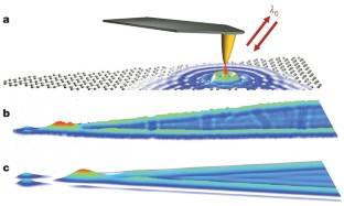
Figure 1: Imaging propagating and localized graphene plasmons by scattering-type SNOM.
The alternative text for this image may have been generated using AI.
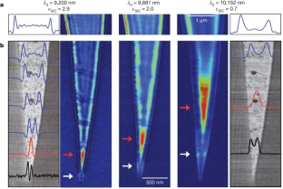
Figure 2: Controlling the plasmon wavelength over a wide range.
The alternative text for this image may have been generated using AI.
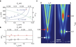
Figure 3: Comparison of theoretical model with experimental results.
The alternative text for this image may have been generated using AI.
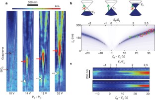
Figure 4: Plasmonic switching and active control of the plasmon wavelength by electrical gating.
The alternative text for this image may have been generated using AI.
References
- Wunsch, B., Stauber, T., Sols, F. & Guinea, F. Dynamical polarization of graphene at finite doping. N. J. Phys. 8, 318 (2006)
Article Google Scholar - Hwang, E. H. &. das Sarma, S. Dielectric function, screening, and plasmons in two-dimensional graphene. Phys. Rev. B 75, 205418 (2007)
Article ADS Google Scholar - Polini, M. et al. Plasmons and the spectral function of graphene. Phys. Rev. B 77, 081411(R) (2008)
Article ADS Google Scholar - Jablan, M., Buljan, H. & Soljačić, M. Plasmonics in graphene at infrared frequencies. Phys. Rev. B 80, 245435 (2009)
Article ADS Google Scholar - Hill, A., Mikhailov, S. A. & Ziegler, K. Dielectric function and plasmons in graphene. Europhys. Lett. 87, 27005 (2009)
Article ADS Google Scholar - Novoselov, K. S. et al. Electric field effect in atomically thin carbon films. Science 306, 666–669 (2004)
Article CAS ADS Google Scholar - Ju, L. et al. Graphene plasmonics for tunable terahertz metamaterials. Nature Nanotechnol. 6, 630–634 (2011)
Article CAS ADS Google Scholar - Fei, Z. et al. Infrared nanoscopy of Dirac plasmons at the graphene–SiO2 interface. Nano Lett. 11, 4701–4705 (2011)
Article CAS ADS Google Scholar - Keilmann, F. & Hillenbrand, R. Near-field microscopy by elastic light scattering from a tip. Phil. Trans. A 362, 787–805 (2004)
Article CAS ADS Google Scholar - Huber, A., Ocelic, N., Kazantsev, D. & Hillenbrand, R. Near-field imaging of mid-infrared surface phonon polariton propagation. Appl. Phys. Lett. 87, 081103 (2005)
Article ADS Google Scholar - Novotny, L. & Hecht, B. Principles of Nano-optics (Cambridge Univ. Press, 2006)
Book Google Scholar - Vakil, A. & Engheta, N. Transformation optics using graphene. Science 332, 1291–1294 (2011)
Article CAS ADS Google Scholar - Koppens, F. H. L., Chang, D. E. & García de Abajo, F. J. Graphene plasmonics: a platform for strong light–matter interactions. Nano Lett. 11, 3370–3377 (2011)
Article CAS ADS Google Scholar - Liu, Y., Willis, R., Emtsev, K. & Seyller, T. Plasmon dispersion and damping in electrically isolated two-dimensional charge sheets. Phys. Rev. B 78, 201403(R) (2008)
Article ADS Google Scholar - Eberlein, T. et al. Plasmon spectroscopy of free-standing graphene films. Phys. Rev. B 77, 233406 (2008)
Article ADS Google Scholar - Zhou, W. et al. Atomically localized plasmon enhancement in monolayer graphene. Nature Nanotechnol 7, 161–165 (2012)
Article CAS ADS Google Scholar - Bostwick, A., Ohta, T., Seyller, T., Horn, K. & Rotenberg, E. Quasiparticle dynamics in graphene. Nature Phys. 3, 36–40 (2007)
Article CAS ADS Google Scholar - Hillenbrand, R., Taubner, T. & Keilmann, F. Phonon-enhanced light matter interaction at the nanometre scale. Nature 418, 159–162 (2002)
Article CAS ADS Google Scholar - Ocelic, N., Huber, A. & Hillenbrand, R. Pseudoheterodyne detection for background-free near-field spectroscopy. Appl. Phys. Lett. 89, 101124 (2006)
Article ADS Google Scholar - Camara, N. et al. Current status of self-organized epitaxial graphene ribbons on the C face of 6H–SiC substrates. J. Phys. D Appl. Phys. 43, 374011 (2010)
Article Google Scholar - Castro Neto, A. H., Peres, N. M. R., Novoselov, K. S. & Geim, A. K. The electronic properties of graphene. Rev. Mod. Phys. 81, 109–162 (2009)
Article CAS ADS Google Scholar - Crassee, I. et al. Multicomponent magneto-optical conductivity of multilayer graphene on SiC. Phys. Rev. B 84, 035103 (2011)
Article ADS Google Scholar - Hofmann, M., Zywietz, A., Karch, K. & Bechstedt, F. Lattice dynamics of SiC polytypes within the bond-charge model. Phys. Rev. B 50, 13401 (1994)
Article CAS ADS Google Scholar - Fei, Z. et al. Gate-tuning of graphene plasmons revealed by infrared nano-imaging. Nature http://dx.doi.org/10.1038/nature11253 (this issue)
- Christensen, J., Manjavacas, A., Thongrattanasiri, S., Koppens, F. H. L. & García de Abajo, F. J. Graphene plasmon waveguiding and hybridization in individual and paired nanoribbons. ACS Nano 6, 431–440 (2012)
Article CAS Google Scholar - Atwater, H. A. The promise of plasmonics. Sci. Am. 296, 56–62 (2007)
Article CAS Google Scholar - Zia, R., Schuller, J. A., Chandran, A. & Brongersma, M. L. Plasmonics: the next chip-scale technology. Mater. Today 9, 20–27 (2006)
Article CAS Google Scholar - Thongrattanasiri, S., Koppens, F. & García de Abajo, F. J. Complete optical absorption in periodically patterned graphene. Phys. Rev. Lett. 108, 047401 (2012)
Article ADS Google Scholar - Hecht, B., Bielefeldt, H., Novotny, L., Inouye, Y. & Pohl, D. W. Local excitation, scattering, and interference of surface plasmons. Phys. Rev. Lett 77, 1889–1892 (1996)
Article CAS ADS Google Scholar - Nikitin, A. Y., Guinea, F., Garcia-Vidal, F. J. & Martín-Moreno, L. Edge and waveguide terahertz surface plasmon modes in graphene microribbons. Phys. Rev. B 84, 161407(R) (2011)
Article ADS Google Scholar
Acknowledgements
We thank L. Novotny, N. van Hulst, R. Quidant and P. Jarillo-Herrero for discussions. This work was supported in part by the Fundacicio Cellex Barcelona, the Spanish MICINN (MAT2010-14885 and Consolider NanoLight.es), the European FP7 projects FP7-HEALTH-F5-2009-241818-NANOANTENNA, FP7-ICT- 2009-4-248909-LIMA and FP7-ICT-2009-4-248855-N4E, the ERC Starting grant no. 258461 (TERATOMO), and the ERC Career integration grant GRANOP.
Author information
Author notes
- Jianing Chen, Michela Badioli, Pablo Alonso-González, Sukosin Thongrattanasiri and Florian Huth: These authors contributed equally to this work.
Authors and Affiliations
- CIC nanoGUNE Consolider, 20018 Donostia-San Sebastián, Spain ,
Jianing Chen, Pablo Alonso-González, Florian Huth & Rainer Hillenbrand - Centro de Fisica de Materiales (CSIC-UPV/EHU) and Donostia International Physics Center (DIPC), 20018 Donostia-San Sebastián, Spain ,
Jianing Chen - ICFO-Institut de Ciéncies Fotoniques, Mediterranean Technology Park, 08860 Castelldefels, Barcelona, Spain ,
Michela Badioli, Johann Osmond, Marko Spasenović & Frank H. L. Koppens - IQFR-CSIC, Serrano 119, 28006 Madrid, Spain ,
Sukosin Thongrattanasiri & F. Javier García de Abajo - Neaspec GmbH, 82152 Martinsried, Munich, Germany ,
Florian Huth - Graphenea SA, 20018 Donostia-San Sebastián, Spain ,
Alba Centeno, Amaia Pesquera & Amaia Zurutuza Elorza - CNM-IMB-CSIC–Campus UAB, 08193 Bellaterra, Barcelona, Spain ,
Philippe Godignon - GREMAN, UMR 7347, Université de Tours/CNRS, 37071 Tours Cedex 2, France ,
Nicolas Camara - IKERBASQUE, Basque Foundation for Science, 48011 Bilbao, Spain ,
Rainer Hillenbrand
Authors
- Jianing Chen
- Michela Badioli
- Pablo Alonso-González
- Sukosin Thongrattanasiri
- Florian Huth
- Johann Osmond
- Marko Spasenović
- Alba Centeno
- Amaia Pesquera
- Philippe Godignon
- Amaia Zurutuza Elorza
- Nicolas Camara
- F. Javier García de Abajo
- Rainer Hillenbrand
- Frank H. L. Koppens
Contributions
J.C., P.A.-G., F.H., F.H.L.K. and R.H. carried out the near-field imaging experiments and participated in data analysis. M.S. participated in data analysis. S.T. and F.J.G.d.A. contributed to the interpretation of the data and developed analytical and computational theoretical tools. N.C., P.G., A.C., A.P. and A.Z.E. provided materials. M.B. and J.O. fabricated the devices. J.G.d.A., R.H. and F.H.L.K. wrote the manuscript.
Corresponding authors
Correspondence toF. Javier García de Abajo, Rainer Hillenbrand or Frank H. L. Koppens.
Ethics declarations
Competing interests
R.H. is co-founder of Neaspec GmbH, a company producing scattering-type scanning near-field optical microscope systems, such as the one used in this study. All other authors declare no competing financial interests.
Supplementary information
PowerPoint slides
Rights and permissions
About this article
Cite this article
Chen, J., Badioli, M., Alonso-González, P. et al. Optical nano-imaging of gate-tunable graphene plasmons.Nature 487, 77–81 (2012). https://doi.org/10.1038/nature11254
- Received: 01 March 2012
- Accepted: 21 May 2012
- Published: 20 June 2012
- Issue date: 05 July 2012
- DOI: https://doi.org/10.1038/nature11254
This article is cited by
Editorial Summary
Voltage-controlled graphene plasmonics
Plasmonic devices, which exploit surface plasmons (electromagnetic waves that propagate along the surface of metals) offer the possibility of controlling and guiding light at subwavelength scales. All eyes are on graphene — atom-thick layers of carbon — as a promising platform for plasmonic applications because it can strongly interact with light and host surface plasmons in the infrared range. Two independent groups reporting in this issue of Nature show that plasmons can be directly launched in graphene, and observed with near-field optical microscopy. Moreover, the wavelengths and amplitudes of the plasmons can be tuned by a gate voltage, a promising capability for the development of on-chip graphene photonics for use in applications including telecommunications and information processing.