Giant spin-accumulation signal and pure spin-current-induced reversible magnetization switching (original) (raw)
In a vertical spin-valve nanopillar consisting of a ferromagnet/non-magnet/ferromagnet trilayer, the magnetic state can be switched between the antiparallel and the parallel configurations by applying a charge current1,2,3,4,5,6,7,8,9,10,11. This charge-current-induced magnetization switching (CIMS) is the result of a direct transfer of spin angular momentum from the spin current carried along the charge current to the localized magnetic moment in the ferromagnet. Separation of the charge and spin components raises the possibility of chargeless pure spin-current-induced magnetization switching (pure spin CIMS).
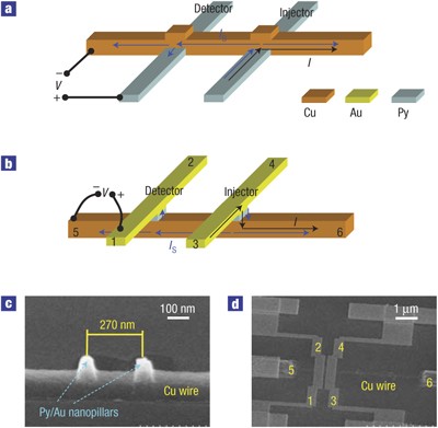
The pure spin current transfers only spin angular momentum, and thus provides an attractive means to manipulate the magnetic state in magnetic nanostructures as well as a quiet electrical background for experimental studies. The pure spin current _I_S can be generated by the diffusion of the accumulated spins12,13,14,15,16,17,18,19,20 in a metallic lateral spin-valve (LSV) structure with non-local electrical spin injection, as shown in Fig. 1a. When the spin accumulation at the interface between the permalloy (Py) and Cu wires on the detector side is non-collinear to the Py magnetization, the transverse component of the pure spin current is absorbed on entering the detector. Therefore, in the absence of a charge current, a spin-transfer torque could still be exerted on the Py magnetization2,18. However, so far, reversible magnetic switching similar to the CIMS has not been achieved by using pure spin currents, mainly because of low spin-injection efficiency. Usually the LSV is fabricated through two separate processes for the ferromagnet and the non-magnet nanowires, which inevitably introduces contamination or oxidation at the ferromagnet/non-magnet interfaces, causing spin-flip scattering and leading to the loss of the spin signal.
Figure 1: Sample structure.
a, Schematic structure of a typical previously reported LSV. b, Schematic structure of our present LSV. c, Scanning electron micrograph taken during fabrication, showing a Cu wire with two Py/Au nanopillars. d, Scanning electron micrograph of the finished sample. The non-local measurement geometry is also shown in a and b, with I being the charge current and _I_S being the spin current. For the sample shown in c and d, the Py nanomagnets in both the detector and the injector nanopillars are 20 nm in thickness. The Cu wire is 170 nm in width and 65 nm in thickness. The in-plane sizes of the two rectangular Py nanomagnets are 80×170 nm2 and 75×170 nm2 respectively, and their long axes are perpendicular to the Cu wire. The spins injected from the Py into the Cu are accumulated at the interface and diffuse, which creates a pure spin current flowing in the Cu wire and into the detector. Spin-dependent conduction in the detector nanomagnet leads to a difference in the electrochemical potential between the Py and Cu terminals. Therefore, a voltage V is measured, which is proportional to the spin accumulation at the Cu/detector interface15.
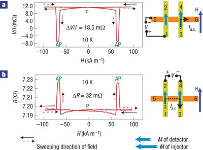
To improve the non-local spin injection efficiency, we have fabricated the newly designed sample shown in Fig. 1b. The injector and the detector are not nanowires but Py(Ni81Fe19)/Au nanopillars whose constituents (Cu, Py and Au) are all deposited successively in the same vacuum, yielding very clean interfaces. The measured non-local spin-valve signal V/I is plotted in Fig. 2a as a function of the magnetic field applied along the easy axis of the Py nanomagnets. The sharp transitions in the non-local spin-valve signal correspond to the magnetic switching of the Py nanomagnets. The higher and the lower values of the non-local spin-valve signal correspond to the parallel and antiparallel states respectively. The difference in the non-local spin-valve signal Δ_V_/I between antiparallel and parallel states is proportional to the spin accumulation in the Cu wire. The observed Δ_V_/I signal is surprisingly large, ranging from 8 to 21 mΩ at 10 K for ten samples fabricated in two batches. At room temperature, Δ_V_/I is reduced to approximately 1/3 of its value at 10 K. These values are an order of magnitude larger than previously reported values in Py/Cu LSVs with the same injector-to-detector separation12,13,15,16. The giant non-local spin-valve signal indicates that giant spin accumulation takes place in the Cu wire, demonstrating high non-local spin injection efficiency. The main reason for this large signal is the improved interface quality between the Py and Cu, which minimizes the interfacial spin-flip scattering that causes a suppression of the spin signal. By solving the spin-diffusion equation21,22, the non-local spin signal is analytically deduced as 20

where P, λ and d are respectively the spin polarization factor, the spin-diffusion length and the centre-to-centre distance between the injector and detector, that is, the 270-nm distance shown in Fig. 1c. _R_S is the spin resistance, defined as R_S=2_ρ λ/[(1−_P_2)S_], with the resistivity ρ and the effective cross-sectional area S. Using the materials parameters determined in our recent experiments20, including the spin-diffusion lengths of 1,000 nm and 5 nm for Cu and Py respectively, Δ_V/I is calculated as being 14.4 mΩ for the sample shown in Fig. 1c,d. Despite some sample-to-sample variation, the experimental results are in good agreement with the theoretical calculation.
Figure 2: Transport measurement results for the sample shown in Fig. 1c,d.
a, Non-local spin-valve signal as a function of magnetic field. b, Local spin-valve signal as a function of magnetic field. AP: antiparallel; P: parallel. The measurement geometry is drawn beside each graph.
According to equation (1), a large value of S causes a reduction of the non-local spin-valve signal Δ_V_/I. Because of the short spin-diffusion length of ∼5 nm, S is the Cu/Py-interface area for Py. As shown in Fig. 1b, in our present structure, S is effectively diminished. In addition, the inhomogeneous spin current distribution observed in our previous LSVs (ref. 15) should be diminished in the present structure. Therefore, in addition to the clean interfaces, our particular structure also contributes to the improved non-local spin signal.
For comparison, the local spin-valve signal measured between contacts 2 and 4 by applying the current between contacts 1 and 3 is shown in Fig. 2b. The anisotropic magneto-resistance effect is visible in the curve. The resistance difference between the antiparallel and parallel states is 32 mΩ, 1.7 times larger than the non-local spin signal, in reasonable agreement with the factor of 2 predicted in ref. 13.
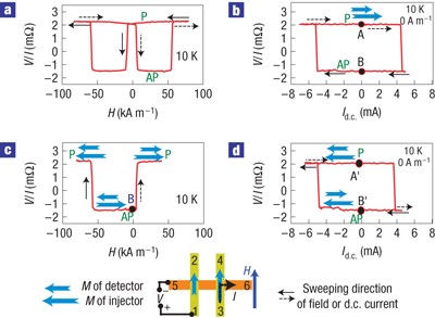
With the benefit of the highly improved non-local spin injection efficiency, we now study magnetization switching induced by a pure spin current. Because the spin transfer occurs near the interface1,23, we reduce the Py thickness of the detector to 4 nm to minimize the spin current necessary for the magnetization switching. Figure 3a shows the non-local spin-valve signal as a function of the external field for such a sample. The values of Δ_V_/I for these samples are around 4 mΩ, smaller than that in Fig. 2a, but still much larger than previously reported values. The lower non-local spin-valve signal is attributed to the fact that the Py thickness is reduced and is comparable to the spin-diffusion length. This decreases the difference in the electrochemical potential between the detector and the Cu wire15. By comparison with the anisotropic magneto-resistance measurements for both the detector and the injector, the higher and lower values of the switching fields are identified as being the switching fields of the Py injector and detector nanomagnets, respectively.
Figure 3: Non-local spin injection results for a sample with 4-nm-thick Py nanomagnet in the detector.
a, Non-local spin-valve signal as a function of magnetic field. b, The non-local spin signal as a function of injected d.c. current. The loop starts at the initial parallel state A. c, The dependence of non-local spin-valve signal on the magnetic field for the antiparallel state B shown in b. d, The same measurement as b, but with an opposite initial parallel state A′. The measurement geometry is drawn below the graphs.
A variable d.c. current is applied between contacts 3 and 6. The sample is preset to a parallel state (denoted A in Fig. 3) at which both magnetizations are aligned in the positive field direction. As can be seen in Fig. 3b, as the d.c. current is increased, the non-local spin-valve signal sharply decreases at about 4.5 mA, indicating a clear magnetization reversal. According to the change in the non-local spin-valve signal, the parallel state is transformed into an antiparallel state (denoted B), which is switched back to the parallel state by a negative d.c. current of −5 mA. Therefore, reversible magnetization switching between antiparallel and parallel states is realized by means of non-local spin injection. Similar results are also observed for other samples.
The magnetic configuration of the antiparallel state B is characterized by applying an external field in either the positive or negative direction. According to the switching-field values shown in Fig. 3c, the magnetic configuration of the antiparallel state B is easily determined, as shown in the figure. The switch from the initial parallel state A to the antiparallel state B is realized by the reversal of the detector magnetization. Therefore, a charge current between contacts 3 and 6 induces switching of the detector magnetization, where there is no charge current. The switching from the antiparallel back to the parallel states is also confirmed to take place through the reversal of the detector magnetization.
As shown in Fig. 3d, for an initial parallel state oriented in the opposite direction, A′, a similar switching loop is measured. In Fig. 3b,d, regardless of the magnetization orientation of the initial parallel state, the parallel-to-antiparallel switching is caused by a positive d.c. current and the antiparallel-to-parallel switching by a negative d.c. current, indicating that the Oersted field hardly affects the magnetization switching. This relationship between the d.c. current direction and the switching direction can be explained only by the spin-transfer theory. Therefore, the current-induced magnetization reversals in Fig. 3b,d are induced by the spin transfer from the pure spin current generated in the non-local geometry, as shown in Fig. 1.
The spin current _I_S flowing into the detector can be derived from the spin-diffusion equation as

with t being the Py thickness of the detector. Using our observed critical switching d.c. current of 5 mA, we calculate the critical spin current for magnetization switching as 317 μA, which is equivalent to a spin current density of approximately 2.5×10¹⁰ A m−2.
When there is a small angle θ between the injector and detector magnetizations, the transverse component (ℏ/2)(I_S/e)sin_θ of the angular momentum carried by the spin current is transferred to the detector. By putting this contribution into the Landau–Lifschitz–Gilbert equation and neglecting the small in-plane uniaxial anisotropy, the critical spin current for the switching between the antiparallel and parallel states is derived as7

Here α is the damping factor, M is the magnetization, _V_vol is the volume of the Py nanomagnet in the detector and _μ_0 is the permeability in vacuum. For Py, α is reported as being between 0.002 and 0.007 (refs 24, 25, 26). By taking _M_=7.8×10⁵ A m−1, the critical spin current density for the switching is calculated as being in the range of 1–3.5×10¹⁰ A m−2, in very good agreement with the estimate from our experimental data. On the other hand, in the previous CIMS experiments, the critical switching charge current density for Py/Cu/Py nanopillars10,27,28 was reported in the range 1×10¹¹–3×10¹¹ A m−2. With a current polarization of ∼0.2, the critical local spin current density for the switching in the CIMS experiments is in the range 2–6×10¹⁰ A m−2. Therefore, our results are theoretically reasonable, and consistent with the reported CIMS results.
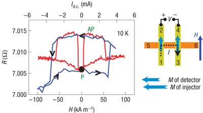
Compared with the Cu spacer thickness in a Py/Cu/Py nanopillar used in the CIMS experiment, which is usually less than 10 nm, the distance d of 270 nm between injector and detector in our sample seems very large. However, because of the long spin-diffusion length of 1,000 nm, the spin signal loss after travelling 270 nm in the Cu wire is only 1−exp(−270/1,000)=24%. Thus, 3/4 of the spin signal, the polarized spin angular momentum, remains. In addition, direct local-injection experiments using the same sample also bring about the CIMS (Fig. 4). This is complementary proof indicating the switching is induced by the spin-transfer effect over the length of 270 nm.
Figure 4: Local spin injection results for the sample described in Fig. 3.
The red line is the field dependence; the blue line is the d.c. current dependence.
The realization of magnetization switching induced by both local and non-local spin injection unifies the up-to-now separate developments of perpendicular nanopillars and lateral magnetic nanostructures. Relative to the previous work18, much more than the improvement in the fabrication process, the high non-local spin injection efficiency and the induced efficient magnetization switching are critical for verifying the theoretical work in these multi-terminal structures2. Obtained with the high-quality multi-terminal structure comprising laterally connected ferromagnetic nanopillars, our present results also confirm that it is possible to realize such novel multi-terminal spintronics devices as the spin-flip transistor and spin-torque transistor2.


