Detective quantum efficiency of electron area detectors in electron microscopy - PubMed (original) (raw)
Detective quantum efficiency of electron area detectors in electron microscopy
G McMullan et al. Ultramicroscopy. 2009 Aug.
Abstract
Recent progress in detector design has created the need for a careful side-by-side comparison of the modulation transfer function (MTF) and resolution-dependent detective quantum efficiency (DQE) of existing electron detectors with those of detectors based on new technology. We present MTF and DQE measurements for four types of detector: Kodak SO-163 film, TVIPS 224 charge coupled device (CCD) detector, the Medipix2 hybrid pixel detector, and an experimental direct electron monolithic active pixel sensor (MAPS) detector. Film and CCD performance was measured at 120 and 300 keV, while results are presented for the Medipix2 at 120 keV and for the MAPS detector at 300 keV. In the case of film, the effects of electron backscattering from both the holder and the plastic support have been investigated. We also show that part of the response of the emulsion in film comes from light generated in the plastic support. Computer simulations of film and the MAPS detector have been carried out and show good agreement with experiment. The agreement enables us to conclude that the DQE of a backthinned direct electron MAPS detector is likely to be equal to, or better than, that of film at 300 keV.
Figures
Fig. 1
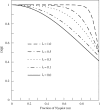
Illustration of the effect on the spatial frequency dependence of the DQE resulting from damping the MTF via deterministic blur. The blur is given by a Gaussian with 1/e length parameter, λ, specified in terms of the pixel pitch (see Section 3). λ=0 corresponds to a perfect pixel detector with no blur and DQE(ω)=sinc2(πω/2). The MTF at the Nyquist frequency varies as (2/π)exp(-π2λ2/4) and the corresponding values with λ equal to 0, 0.1, 0.3, 0.5 and 1.0 are 63.7%, 62.1%, 51.0%, 34.4% and 5.4%, respectively.
Fig. 2
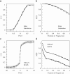
Illustration of ESF and MTF calculations. (a) shows the calculated ESF (solid) from a simulated image of a perfect pixel detector and the corresponding fits based on models using a single Gaussian (dashed). The fit obtained using a single Gaussian with sinc correction is not shown as it is indistinguishable from the calculated ESF result. (b) shows the MTF results of a perfect detector sinc((π/2)ω) MTF (solid) and that obtained from the single Gaussian fit (dashed). The MTF of the single Gaussian with sinc correction is indistinguishable from the perfect detector result. (c) shows the calculated ESF (grey) calculated from the measured 300 keV edge image of the MAPS detector and corresponding fit based on a double Gaussian model (dashed). (d) compares the calculated MTF obtained from the double Gaussian fit (dashed) and double Gaussian fit with sinc correction (solid). Also shown (but offset by -0.25 vertically) is a comparison of the MTF from the double Gaussian fit (dashed) and that calculated via the numerical differentiation of the ESF (solid).
Fig. 3
(a) Illustration of the noise binning method for calculating DQE(0) by plotting the estimated noise, Sn2/n2, as a function of n-fold binning. Results (black circles) are from the difference between successive images captured on the MAPS detector at 300 keV. The plateau value of 1.97×10⁶ illustrated by the horizontal dot-dashed line represents twice the noise per pixel. The average signal was 1770 and there were 7.9 electrons per pixel and so DQE(0)=17702/(121.97×106)/7.9=0.40. (b) shows the calculated DQE(ω) of the MAPS detector at 300 keV along with the N(ω) and MTF2(ω) illustrating the origin of the spatial frequency dependence of DQE. DQE(ω) was calculated using Eq. (6) and the value at ω=0 calculated independently in (a) is indicated (∘).
Fig. 4
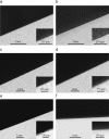
Shadow image of the edge of 0.5 mm gold wire. (a) SO-163 film after exposure to 120 keV electrons, 6μm pixel, 19 electrons/pixel, (b) SO-163 film after exposure to 300 keV electrons, 6μm pixel, 24 electrons/pixel, (c) TVIPS 224 CCD detector, 120 keV electrons, 24μm pixel, 104 electrons/pixel, (d) TVIPS 224 CCD detector, 300 keV electrons, 24μm pixel, 134 electrons/pixel, (e) Medipix2/Quad, 120 keV electrons, 55μm pixel, 3800 electrons/pixel; four dead pixels are visible, and (f) MAPS, 300 keV electrons, 25μm pixel, 24000 electrons/pixel.
Fig. 5
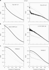
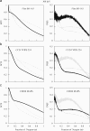
MTF (left) and DQE(ω) (right) calculated from the 120 keV images in Fig. 4 for (a) Kodak SO-163 film, (b) TVIPS 224 and (c) Medipix2 detectors. The indicated detectors results are shown in black but to aid comparison the corresponding results for the other detectors are shown in grey.
Fig. 6
MTF (left) and DQE(ω) (right) calculated from the 300 keV images in Fig. 4 for (a) Kodak SO-163 film using a cut-away holder, (b) TVIPS 224 and (c) MAPS detectors. The indicated detectors results are shown in black but to aid comparison the corresponding results for the other detectors are shown in grey.
Fig. 7
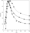
Measured average signal per electron as a function of incident electron energy for TVIPS 224 CCD (■), SO-163 film (•), MAPS (♦) detector. The results have been arbitrarily scaled to have a peak value of ∼100. The lines through the data points are simply aids to the eye. The shape of the response curve is similar for all three detectors. Extrapolating to zero response gives threshold energies of 5, 8 and 24 keV for the CCD, film and MAPS detectors, respectively.
Fig. 8
Calculation of the Medipix2 DQE at 120 keV using the statistics of individual electron events. (a) shows the total number of events (•) recorded per frame and the composition in terms of events recorded in a given number of pixels, as a function of the energy threshold. A total of 2100 electrons were expected per frame. For a threshold of one half the incident energy only single pixel events are seen and at 120 keV no events were seen involving six or more pixels even with a very low threshold. (b) shows the DQE calculated using DQE(0)=(∑iiNi)2/[(∑ii2Ni)(∑iNi)], where Ni is the number of events in each frame where a single electron is counted in i adjacent pixels. Also shown is the corresponding DQE at Nyquist calculated using Eq. (6).
Fig. 9
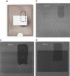
Images showing the effects at different incident electron energies of both electron backscattering from the metal film holder and from light generated within the plastic film backing due to the passage of high energy electrons in Kodak SO-163 film. (a) Photograph of a film holder showing the cut-away region in the centre. The area where black ink was applied to the back of the sheet of film to suppress light reflection is indicated by the dashed box. (b) Image taken with 120 keV electrons showing the area around the cut-away film holder. The OD in the area where the ink was applied is ∼2% lower (the developed film is lighter in the area where the ink was applied). At 120 keV there is no sign of any effects from the film holder. (c) Image taken with 200 keV electrons showing a reduction in OD of ∼9% with the ink and a ∼4% reduction where there is no film holder and so no electron backscatter from the film holder. (d) Image taken with 300 keV electrons showing a ∼10% reduction in OD with the ink and a ∼15% reduction in OD from the removal of electron backscatter.
Fig. 10
(a) The measured MTF at 300 keV for SO-163 film showing the effects of electron backscattering from the metal holder and light generated in the plastic backing: dashed line is the MTF obtained with an unmodified holder; the dotted line is with the metal backing removed; the solid line is with both the metal backing removed and ink applied to suppress light reflection off the bottom of the film. The inset in (a) shows the measured ESF used in calculating the solid line. (b) The measured DQE for SO-163 film as a function of spatial frequency with (grey) and without (black) the metal holder.
Fig. 11
Comparison of measured spatial frequency variation of the MTF of SO-163 at 20, 50, 120, 200 and 300 keV. The images were scanned with a 6μm step. At 300 keV, results for a normal holder, cut-away holder and cut-away holder with light absorbing ink are shown. The MTF of the densitometer has not been corrected for and so the intrinsic MTF values for film at Nyquist will be about twice that shown here. Note how the minimum MTF at Nyquist occurs at the energy giving the maximum response per incident electron (see Fig. 7).
Fig. 12
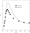
Comparison of measured and simulated OD in response to one electron per μm2 as a function of incident energy for SO-163 film.
Fig. 13
Monte Carlo simulation results for SO-163 film: (a) MTF at 120 keV; (b) DQE(ω) at 120 keV; (c) MTF at 300 keV; and (d) DQE(ω) at 300 keV. Results corresponding to SO-163 film in a normal film holder are shown in black. The effect of electron backscattering is illustrated by showing results obtained with a backless film holder using ♢ and for backthinned film (in which there is also no plastic support for the emulsion) in grey.
Fig. 14
Schematic of MAPS CMOS detector. The pixel spacing is determined by the spacing between diodes formed by the N well doped areas indicated in blue. The division into three layers used in the simulations is indicated and consists of: (a) passivation and heavily doped wells; (b) sensitive layer consisting of the lightly doped epilayer; and (c) heavily doped substrate. The track of an incident electrons is shown illustrating the problem with backscattering from the substrate in a non-backthinned detector. The diffusive collection by the reverse biased N well diodes of mobile electrons generated in electron-hole pair excitations is indicated.
Fig. 15
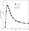
Calculated average energy per incident electron deposited within the sensitive layer of the MAPS CMOS detector as a function of incident energy using—CSDA approximation and … the FMC. The measured results, indicated by the solid circles, have been scaled from the raw ADC values.
Fig. 16
(a) Solid lines show the calculated deposited energy density as a function of radius for incident 300 keV electrons on the 3-layer (black) and 2-layer, i.e., backthinned, models for the MAPS detector. The dotted lines show the cumulative integrals of the corresponding point spread functions as a function of radius. By definition these must equal unity for large radius. (b) Comparison of measured (∘) and various calculated MTF results for MAPS detector at 300 keV. The MTF calculated from the PSF and an edge simulation are shown as solid and dashed lines, respectively. The backthinned MTF is shown in grey. The calculated edge MTF multiplied by exp(-0.26ω2) is indistinguishable from the measured MTF.
Fig. 17
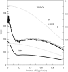
Comparison of measured and calculated spatial frequency variation of the DQE for a MAPS detector at 300 keV. The measured DQE is indicated by the circles (∘) while the results of calculations using both the CSDA and FMC approximations for non-backthinned (black) detectors and backthinned (grey) detectors are shown. The non-backthinned CSDA calculation results are in very good agreement with the measured results. The backthinned CSDA are within ∼90% of those for a perfect and plotted against the right hand axes. The corresponding FMC results are less than the measured results. Note that the value of DQE(0) for a backthinned detector is less than that for a non-backthinned detector. The backthinned detectors do not show the drop with increasing ω due to backscattering.
Fig. 18
Calculated probability distributions obtained using the (a) CSDA and (b) FMC models for depositing energy E in a MAPS detector by an incident 300 keV electron. The results for backthinned (grey) and non-backthinned (black) detectors are shown. The dotted vertical lines indicate the position of the corresponding mean energy loss. The dashed line in the FMC calculation indicates the 1/E2 energy dependence of the inelastic Rutherford cross-section.
Fig. 19
(a) Comparison of the measured (∘)DQE(ω) at 300 keV of the MAPS detector with the results of calculations using the FMC (dashed) and the clamped FMC approximations (solid) described in text. The dotted line gives the calculated FMC clamped DQE(ω) for a detector backthinned (by the removal of the substrate) to a total thickness of 35μm. (b) Comparison of the probability distributions for the signal collected from a single incident 300 keV electron, obtained using the FMC approximation energy loss and the corresponding clamped FMC approximation.
Similar articles
- Electron imaging with Medipix2 hybrid pixel detector.
McMullan G, Cattermole DM, Chen S, Henderson R, Llopart X, Summerfield C, Tlustos L, Faruqi AR. McMullan G, et al. Ultramicroscopy. 2007 Apr-May;107(4-5):401-13. doi: 10.1016/j.ultramic.2006.10.005. Epub 2006 Nov 13. Ultramicroscopy. 2007. PMID: 17140733 - Experimental observation of the improvement in MTF from backthinning a CMOS direct electron detector.
McMullan G, Faruqi AR, Henderson R, Guerrini N, Turchetta R, Jacobs A, van Hoften G. McMullan G, et al. Ultramicroscopy. 2009 Aug;109(9):1144-7. doi: 10.1016/j.ultramic.2009.05.005. Epub 2009 May 18. Ultramicroscopy. 2009. PMID: 19541421 Free PMC article. - Electronic detectors for electron microscopy.
Faruqi AR, McMullan G. Faruqi AR, et al. Q Rev Biophys. 2011 Aug;44(3):357-90. doi: 10.1017/S0033583511000035. Epub 2011 Apr 28. Q Rev Biophys. 2011. PMID: 21524337 Review. - Characterization of a Timepix detector for use in SEM acceleration voltage range.
Denisov N, Jannis D, Orekhov A, Müller-Caspary K, Verbeeck J. Denisov N, et al. Ultramicroscopy. 2023 Nov;253:113777. doi: 10.1016/j.ultramic.2023.113777. Epub 2023 Jun 8. Ultramicroscopy. 2023. PMID: 37336162 - Electronic detectors for electron microscopy.
Faruqi AR, Henderson R. Faruqi AR, et al. Curr Opin Struct Biol. 2007 Oct;17(5):549-55. doi: 10.1016/j.sbi.2007.08.014. Epub 2007 Oct 29. Curr Opin Struct Biol. 2007. PMID: 17913494 Review.
Cited by
- Single-Particle Cryo-EM at Crystallographic Resolution.
Cheng Y. Cheng Y. Cell. 2015 Apr 23;161(3):450-457. doi: 10.1016/j.cell.2015.03.049. Cell. 2015. PMID: 25910205 Free PMC article. Review. - Beam-induced motion of vitrified specimen on holey carbon film.
Brilot AF, Chen JZ, Cheng A, Pan J, Harrison SC, Potter CS, Carragher B, Henderson R, Grigorieff N. Brilot AF, et al. J Struct Biol. 2012 Mar;177(3):630-7. doi: 10.1016/j.jsb.2012.02.003. Epub 2012 Feb 16. J Struct Biol. 2012. PMID: 22366277 Free PMC article. - Electron tomography in life science.
Bárcena M, Koster AJ. Bárcena M, et al. Semin Cell Dev Biol. 2009 Oct;20(8):920-30. doi: 10.1016/j.semcdb.2009.07.008. Epub 2009 Aug 5. Semin Cell Dev Biol. 2009. PMID: 19664718 Free PMC article. Review. - Laser-free GHz stroboscopic transmission electron microscope: Components, system integration, and practical considerations for pump-probe measurements.
Lau JW, Schliep KB, Katz MB, Gokhale VJ, Gorman JJ, Jing C, Liu A, Zhao Y, Montgomery E, Choe H, Rush W, Kanareykin A, Fu X, Zhu Y. Lau JW, et al. Rev Sci Instrum. 2020 Feb 1;91(2):021301. doi: 10.1063/1.5131758. Rev Sci Instrum. 2020. PMID: 32113442 Free PMC article. - Gradient-based high precision alignment of cryo-electron subtomograms.
Xu M, Alber F. Xu M, et al. IEEE Int Conf Systems Biol. 2011:279-284. doi: 10.1109/ISB.2011.6033166. IEEE Int Conf Systems Biol. 2011. PMID: 25068871 Free PMC article.
References
- Henderson R. Ultramicroscopy. 1992;46:1–18. - PubMed
- Typke D., Gilpin C.J., Downing K.H., Glaeser R.M. Ultramicroscopy. 2007;107:106–115. - PubMed
- McMullan G., Faruqi A.R. Nucl. Instrum. Meth. A. 2008;591:129–133.
- Medipix2 Collaboration, URL 〈http://medipix.web.cern.ch/MEDIPIX〉.
Publication types
LinkOut - more resources
Full Text Sources
Other Literature Sources
Miscellaneous
