Synthetic nanoelectronic probes for biological cells and tissues - PubMed (original) (raw)
Review
Synthetic nanoelectronic probes for biological cells and tissues
Bozhi Tian et al. Annu Rev Anal Chem (Palo Alto Calif). 2013.
Abstract
Research at the interface between nanoscience and biology could yield breakthroughs in fundamental science and lead to revolutionary technologies. In this review, we focus on the interfaces between nanoelectronics and biology. First, we discuss nanoscale field effect transistors (nanoFETs) as probes to study cellular systems; specifically, we describe the development of nanoFETs that are comparable in size to biological nanostructures involved in communication through synthesized nanowires. Second, we review current progress in multiplexed extracellular sensing using planar nanoFET arrays. Third, we describe the designs and implementation of three distinct nanoFETs used to perform the first intracellular electrical recording from single cells. Fourth, we present recent progress in merging electronic and biological systems at the three-dimensional tissue level by use of macro-porous nanoelectronic scaffolds. Finally, we discuss future developments in this research area, unique challenges and opportunities, and the tremendous impact these nanoFET-based technologies might have on biological and medical sciences.
Figures
Figure 1. FET basics and electrical interfaces between nanoFET and biological systems
(a) Schematic of a planar FET device. In FET, current flows along a semiconductor path called the channel. At one end of the channel, there is an electrode called the source. At the other end of the channel, there is an electrode called the drain. The third electrode that applies a voltage to the channel is called gate, which modulates the electron/hole carrier density and the output of the FET devices. A small voltage change in gate signal can cause a large variation in the current from the source to the drain. This is how FET works and in particular, amplifies signals. (b-c) Schematics of electrically based cellular sensing using a kinked nanoFET, where intracellular potentials (b) or extracellular field potentials (c) can be used to change the nanoFET conductace, analogous to applying a voltage using a gate electrode.
Figure 2. Semiconductor nanowire structural motifs for nanoFETs
(a) Schematics of 1D (I), 2D (II) and 3D (III) motifs. 1D motif (I) can have uniform composition and doping (I, left) or axially (I, middle) or radially (I, right) modulated. A kinked nanowire with structurally coherent “kinks” introduced in a controlled manner during axial elongation represents an example of 2D motif (II). Heterobranched nanowires yield 3D structure (III) and the branch junction (e.g., blue/yellow segment junction) can be exploited for localized sensing. (b) An axial nanowire heterostructure made by modulation in VLS/VSS growth mechanisms. (c) A multiply kinked nanowire showing a probe structure. Yellow and magenta stars denote _cis_- and _trans_- conformations, respectively.
Figure 3. Multiplexed extracellular electrical recordings using nanoFETs
(a) Optical image of a cortical neuron interfaced to three of the four functional nanoFETs in an array. (b) upper panel, optical micrograph showing three nanoFET devices (NW1, NW2, and NW3) in a linear array, where pink indicates the area with exposed NW devices. Lower panel, a differential interference contrast bright field image showing individual cardiomyocytes (purple) and single nanoFETs (yellow). (c) Optical image of an acute slice over a 4 × 4 NWFET array. Signals were recorded simultaneously from the eight devices indicated on the image. Crosses along the LOT fiber region of the slice mark the stimulation spots a–h. The stimulator insertion depth was not controlled precisely in these experiments. (d) Maps of the relative signal intensity or activity for devices 1–8.
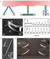
Figure 4. Intracellular electrical recordings using nanoFETs
(a) Schematics of kinked nanoFET (left), BIT-FET (middle) and ANTT (right) probes. (b) SEM image of a kinked nanoFET probe (I) and its intracellular electrical recordings (II, III) from spontaneously beating cardiomyocytes. (c) SEM of a BIT-FET probe, insets highlight the tip and root parts of the hollow branch. (d) SEM image of ANTT probe array.
Figure 5. A comparison between kinked nanoFET probe (a) and conventional intracellular tools (b–d)
The green arrows in (a–d) indicate the current flows. Rs, series resistance; Rj, junction resistance; Rm, membrane resistance; Vm, intracellular potential; Cj, junction capacitance; Cm, membrane capacitance.
Figure 6. Integrating nanoelectronics with cells and tissue
Conventional bulk electronics are distinct from biological systems in composition, structural hierarchy, mechanics and function. Their electrical coupling at the tissue/organ level is usually limited to the tissue surface, where only boundary or global information can be gleaned unless invasive approaches are used. (a) A new concept was introduced where an integrated system can be created from discrete electronic and biological building blocks (for example, semiconductor nanowires, molecular precursors of polymers and single cells). Three biomimetic and bottom-up steps have been designed: step A, patterning, metallization and epoxy passivation for single-nanowire FETs; step B, forming 3D nanowire FET matrices (nanoelectric scaffolds) by self or manual organization and hybridization with traditional ECMs; step C, incorporation of cells and growth of synthetic tissue through biological processes. Yellow dots: nanowire components; blue ribbons: metal and epoxy interconnects; green ribbons: traditional ECMs; pink: cells. (b) Rationale and approaches for biomimetic implementation of nanoelectronics innervated synthetic tissues. A, B and C are the same steps used in (a). (c) The new electronic scaffold component in synthetic tissues enables additional interactions with traditional cellular scaffold and cells.
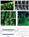
Figure 7. NanoES and synthetic tissues
(a) 3D reconstructed confocal fluorescence micrographs of reticular nanoES. The scaffold was labelled with rhodamine 6G. Solid and dashed open magenta squares indicate two nanowire FET devices located on different planes. (b) SEM image of a loosely packed mesh nanoES, showing the macroporous structure. (c) Confocal fluorescence micrographs of a synthetic cardiac patch. (II and III), Zoomed-in view of the upper and lower dashed regions in I, showing metal interconnects, the SU-8 scaffold (arrows in II) and electrospun PLGA fibres (arrows in III). (d) Epi-fluorescence micrograph of the surface of the cardiac patch. Green (Alexa Fluor 488): α-actin; blue (Hoechst 34580): cell nuclei. The position of the source–drain electrodes is outlined with dashed lines. (e) Conductance versus time traces recorded from a single-nanowire FET before (black) and after (blue) applying noradrenaline. (f) Multiplex electrical recording of extracellular field potentials from four nanowire FETs in a mesh nanoES. Data are conductance versus time traces of a single spike recorded at each nanowire FET.
Similar articles
- Nanoelectronics meets biology: from new nanoscale devices for live-cell recording to 3D innervated tissues.
Duan X, Lieber CM. Duan X, et al. Chem Asian J. 2013 Oct;8(10):2304-14. doi: 10.1002/asia.201300630. Epub 2013 Aug 15. Chem Asian J. 2013. PMID: 23946279 Free PMC article. Review. - Design and synthesis of diverse functional kinked nanowire structures for nanoelectronic bioprobes.
Xu L, Jiang Z, Qing Q, Mai L, Zhang Q, Lieber CM. Xu L, et al. Nano Lett. 2013 Feb 13;13(2):746-51. doi: 10.1021/nl304435z. Epub 2013 Jan 7. Nano Lett. 2013. PMID: 23273386 Free PMC article. - Three-dimensional, flexible nanoscale field-effect transistors as localized bioprobes.
Tian B, Cohen-Karni T, Qing Q, Duan X, Xie P, Lieber CM. Tian B, et al. Science. 2010 Aug 13;329(5993):830-4. doi: 10.1126/science.1192033. Science. 2010. PMID: 20705858 Free PMC article. - Nano-Bioelectronics.
Zhang A, Lieber CM. Zhang A, et al. Chem Rev. 2016 Jan 13;116(1):215-57. doi: 10.1021/acs.chemrev.5b00608. Epub 2015 Dec 21. Chem Rev. 2016. PMID: 26691648 Free PMC article. Review. - Nanoelectronics-biology frontier: From nanoscopic probes for action potential recording in live cells to three-dimensional cyborg tissues.
Duan X, Fu TM, Liu J, Lieber CM. Duan X, et al. Nano Today. 2013 Aug 1;8(4):351-373. doi: 10.1016/j.nantod.2013.05.001. Nano Today. 2013. PMID: 24073014 Free PMC article.
Cited by
- Living myofibroblast-silicon composites for probing electrical coupling in cardiac systems.
Rotenberg MY, Yamamoto N, Schaumann EN, Matino L, Santoro F, Tian B. Rotenberg MY, et al. Proc Natl Acad Sci U S A. 2019 Nov 5;116(45):22531-22539. doi: 10.1073/pnas.1913651116. Epub 2019 Oct 17. Proc Natl Acad Sci U S A. 2019. PMID: 31624124 Free PMC article. - Neural Recording and Modulation Technologies.
Chen R, Canales A, Anikeeva P. Chen R, et al. Nat Rev Mater. 2017 Feb;2(2):16093. doi: 10.1038/natrevmats.2016.93. Epub 2017 Jan 4. Nat Rev Mater. 2017. PMID: 31448131 Free PMC article. - Talking to cells: semiconductor nanomaterials at the cellular interface.
Rotenberg MY, Tian B. Rotenberg MY, et al. Adv Biosyst. 2018 Apr;2(4):1700242. doi: 10.1002/adbi.201700242. Epub 2018 Feb 26. Adv Biosyst. 2018. PMID: 30906852 Free PMC article. - Nanotools for neuroscience and brain activity mapping.
Alivisatos AP, Andrews AM, Boyden ES, Chun M, Church GM, Deisseroth K, Donoghue JP, Fraser SE, Lippincott-Schwartz J, Looger LL, Masmanidis S, McEuen PL, Nurmikko AV, Park H, Peterka DS, Reid C, Roukes ML, Scherer A, Schnitzer M, Sejnowski TJ, Shepard KL, Tsao D, Turrigiano G, Weiss PS, Xu C, Yuste R, Zhuang X. Alivisatos AP, et al. ACS Nano. 2013 Mar 26;7(3):1850-66. doi: 10.1021/nn4012847. Epub 2013 Mar 20. ACS Nano. 2013. PMID: 23514423 Free PMC article. Review. - Nanoscale Semiconductor Devices as New Biomaterials.
Zimmerman J, Parameswaran R, Tian B. Zimmerman J, et al. Biomater Sci. 2014 May 1;2(5):619-626. doi: 10.1039/C3BM60280J. Epub 2014 Jan 9. Biomater Sci. 2014. PMID: 27213041 Free PMC article.
References
- Ieong M, Doris B, Kedzierski J, Rim K, Yang M. Silicon device scaling to the sub-10-nm regime. Science (New York, N.Y.) 2004;306:2057–2060. - PubMed
- Lu W, Lieber CM. Semiconductor nanowires. Journal of Physics D-Applied Physics. 2006;39:R387–R406.
- Lu W, Lieber CM. Nanoelectronics from the bottom up. Nature Materials. 2007;6:841–850. - PubMed
Publication types
MeSH terms
LinkOut - more resources
Full Text Sources
Other Literature Sources


