The Design of Low Noise Amplifiers in Nanometer Technology for WiMAX Applications (original) (raw)
The Design of Low Noise Amplifiers in Nanometer Technology for WiMAX Applications
Kavyashree.P*, Dr. Siva S Yellampalli**
*M.Tech (VLSI Design), VTU Extension Centre, UTL Technologies Limited, Bangalore, India
** Professor, VTU Extension Centre, UTL Technologies Limited, Bangalore, India
Abstract
In this paper the design of two low noise amplifiers proposed for WiMAX applications is presented. The two low noise amplifier topologies implemented are: (1) cascoded common source amplifier, (2) Shunt feedback amplifier. The amplifiers are implemented in a standard 180 nm CMOS process, and are operated with a 1−V1-\mathrm{V} supply voltage and 5.9 GHz frequency, the cascoded LNA achieved the best performance with a simulated gain of 15.7 dB and noise figure of 1.85 dB . The Low noise amplifier has been simulated using cadence spectre.
Index Terms-CMOS; Low-noise-amplifier (LNA); WiMAX
I. InTRODUCTION
The rapid advancement in CMOS scaling and RF CMOS circuit design techniques in the past few years have made it possible to integrate all the elements of a transceiver on a single chip. Inexpensive CMOS technologies have been used successfully to implement all the necessary RF functionality for existing and emerging wireless area network standards, such as Bluetooth and WiMAX [1] [2].The CMOS system-on-chip (SOC) solution to enable a single chip phone, where the analog and digital basebands, power management, and the RF transceiver are fully integrated on a single monolithic CMOS Integrated circuit.
WiMAX is a telecommunications technology which stands for Worldwide Interoperability for Microwave Access. It belongs to the IEEE 802.16 family of standards, which aim to provide wireless broadband access. It provides data rates of up to 100 Mbps at 20 MHz bandwidth [3]. It has a very large coverage area of around 50 km . for one base station which makes it a viable option for implementation of last-mile connectivity. There are two types of WiMAX systems: Fixed WiMAX and Mobile WiMAX. The fixed WiMAX system does not allow handoff between base stations. Mobile WiMAX on the other hand provides both mobile and fixed services.
II. LOW NOISE AMPLIFIERS
The low noise amplifier (LNA) is the vital component in the receiver chain of the communication system. It is the first gain stage behind the antenna in the receiver chain and its noise figure is directly added to the whole system. The LNAs are used to amplify the very weak signals coming from the antenna.
A. Cascoded Common Source Amplifier
The most frequently used topology for LNA design is the cascoded common source amplifier with inductive source degeneration show in the Fig. 1[4]. The cascoded common
source amplifier is also called as telescopic cascode amplifier because the cascode transistor is the same type as the input transistor [5].
The cascode topology gives a higher gain, due to the increase in the output impedance and it also has a better isolation between the input and output ports. The cascode common source amplifier has a higher reverse isolation [6]. The suppression of the parasitic capacitances of the input transistor also improves the higher frequency operation of the amplifier.
B. Shunt Feedback Amplifier
The shunt feedback low noise amplifier is show in the Fig. 4[4]. It has some attractive benefits, like supporting input and output match over a large frequency range and it is able to achieve a very high linearity. The linearity of the amplifier improves the gain, which is largely set feedback, becomes less sensitive to the gain of the amplifier. The feedback elements, which are composed of a resistor in series with a capacitor, linearize the gain and increase the bandwidth of the amplifier. The feedback is also suited for the CMOS low noise amplifiers since the input impedance of MOSFETs is large and mostly capacitive, which means that the input impedance can be controlled and set by the feedback. To improve the high frequency performance, an additional inductor can be positioned in series with the resistor and capacitor [7]. Finally, the high self resonance frequency of inductors, enabled by a post processing technique, has been exploited to achieve a wideband, high impedance drain load.
III. CIRCUIT DESIGNS
The performance requirement for a WiMAX receiver is listed in Table I. These receiver specifications are obtained from the IEEE 802.16 standard released in 2004 [8]. The next part of the design involves the mapping of the specifications from the IEEE standard to relevant system level parameters such as Bit Error Ratio (BER), Signal to noise ratio (SNR), and receiver sensitivity. These system level specifications are then mapped into block level using link budget analysis [9].
Table II. Summarizes the block level specifications for the low noise amplifier. The LNA must be able to achieve high gain and low noise figure to relax the gain requirement of the mixer and at the same time give the whole receiver a low noise figure. The noise figure also determines the minimum input signal that can be resolved by the LNA while the linearity dictates the maximum input signal level that will not cause nonlinear operation. The LNA, having a finite reverse isolation and being connected directly to the antenna, needs a good input and output match to
prevent signals from leaking back to the antenna and getting retransmitted causing unwanted interference.
TABLE I. WiMAX receiver requirements and specifications
| Rx max input level on channel reception tolerance | ≥−30dBm\geq-30 \mathrm{dBm} |
|---|---|
| Rx max input level on channel damage tolerance | ≥0dBm\geq 0 \mathrm{dBm} |
| 1st adjacent channel rejection | ≥4dBm\geq 4 \mathrm{dBm} |
| 2st adjacent channel rejection | ≥23dBm\geq 23 \mathrm{dBm} |
| Image rejection | ≥60dBm\geq 60 \mathrm{dBm} |
| Noise Figure | ≤7 dB\leq 7 \mathrm{~dB} |
TABLE II. Low Noise Amplifier Specifications
| Parameter | LNA Design |
|---|---|
| Technology | 180 nm |
| Frequency | 5.9 GHz |
| Gain | >15 dB>15 \mathrm{~dB} |
| Power Dissipation | <4 mW<4 \mathrm{~mW} |
| Noise Figure | <3 dB<3 \mathrm{~dB} |
| S12 (dB) | −45.86-45.86 |
| S11 (dB) | -10.3 |
| S22 (dB) | -14.5 |
A. Cascoded Common Source Amplifier
In schematic of the designed cascoded common source amplifier is shown in Fig. 1. The input impedance of the cascoded common source low noise amplifier circuit shown in Fig. 1 will be capacitive due to the gate source capacitance Cgs\mathrm{C}_{\mathrm{gs}}. To reduce the noise and improve the power gain in the circuit a lossless degenerating inductor Ls\mathrm{L}_{\mathrm{s}} is added to the source of the cascode transistor M1\mathrm{M}_{1}. The input impedance of the LNA can be computed based on (1) [4], with the value of source inductance Ls\mathrm{L}_{\mathrm{s}}. The width of the cascode transistor M2\mathrm{M}_{2}, was set equal to the width of the input transistor to take advantage of the reduced junction capacitance in the layout. The output matching network, composed of the drain inductor, Ld\mathrm{L}_{\mathrm{d}}, and the output capacitors, C1\mathrm{C}_{1} and C2\mathrm{C}_{2}, can be designed. Fig. 2 shows the final simulation design of the cascoded common source LNA with device sizes and bias voltages. Fig. 3 shows the layout design of cascoded common source LNA [10].
Zin =(fmCgs)∗ Ls\mathrm{Z}_{\text {in }}=\left(\frac{\mathrm{f}_{\mathrm{m}}}{\mathrm{C}_{\mathrm{gs}}}\right) * \mathrm{~L}_{\mathrm{s}}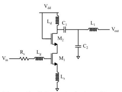
Figure 1. Schematic design of cascoded common source LNA
Figure 2. Simulation setup to analyse the design of cascoded common source LNA
Figure 3. Layout design of cascoded common source LNA
B. Shunt Feedback Amplifier
The design of shunt feedback low noise amplifier is shown in Fig. 4, the value of the feedback resistor which sets the power gain is given in (2) [4], where Rf,ZoR_{f}, Z_{o}, and S21S_{21} are the values of the feedback resistor, output impedance, and the transducer gain. A small inductor was placed in the gate of the transistor to aid input matching. A load inductor was placed in the drain of the transistor to tune out the junction capacitances in the drain of the transistor. The value of the feedback capacitor, which is used for biasing purposes, was set large enough to not have a significant effect on feedback. The Fig. 5 and Fig. 6 shows the simulation and the layout design of the shunt feedback LNA.
Rf=Zo(1+∣S21∣)\mathrm{R}_{\mathrm{f}}=\mathrm{Z}_{\mathrm{o}}\left(1+\left|\mathrm{S}_{21}\right|\right).
Figure 4. Schematic design of shunt feedback LNA

Figure 5. Simulation setup to analyse the design of shunt feedback LNA
Figure 6. Layout design of shunt feedback LNA
IV. CALCULATION AND ANALYSIS
The LNA topologies were implemented in a standard 180- nm CMOS process. The extraction of all device parameters for use in simulations was done using Virtuoso Schematic Composer and Spectre Simulator from Cadence Design System. The low-noise amplifiers were designed to operate at the frequency band of 5.725 GHz to 5.925 GHz and the measurements in the plots were taken at 5.9 GHz .
A. Inductive Source Degeneration Input Matching
The first constraint on the LNA was to assure that the input impedance matches the source impedance, i.e. the LNA presents a purely resistive load of 50Ω50 \Omega to the antenna, in order to maximize the power transfer.
Figure 7. Schematic of a cascode LNA design with source degeneration
Figure 8. Equivalent model with source degeneration
Zin =VgIg=IgRg+Vc+jωIsLsIg\mathrm{Z}_{\text {in }}=\frac{\mathrm{V}_{\mathrm{g}}}{\mathrm{I}_{\mathrm{g}}}=\frac{\mathrm{I}_{\mathrm{g}} \mathrm{R}_{\mathrm{g}}+\mathrm{V}_{\mathrm{c}}+\mathrm{j} \omega \mathrm{I}_{\mathrm{s}} \mathrm{L}_{\mathrm{s}}}{\mathrm{I}_{\mathrm{g}}}
Zin =Ls⋅gmcgg\mathrm{Z}_{\text {in }}=\frac{\mathrm{L}_{\mathrm{s}} \cdot \mathrm{g}_{\mathrm{m}}}{\mathrm{c}_{\mathrm{gg}}} where Zin \mathrm{Z}_{\text {in }} may be say 50 ohms
In most LNA designs the value of Ls is picked and the values of gm and Cgs are calculated to give the required Zin \mathrm{Z}_{\text {in }}.
B. Degeneration Inductor LSL_{S}
The value of this inductor is fairly arbitrary but is ultimately limited on the maximum size of inductance allowed by the technology.
ωT=gmcgs=RsLs=501nH=50GHz\omega_{\mathrm{T}}=\frac{\mathrm{gm}}{\mathrm{cgs}}=\frac{\mathrm{R}_{\mathrm{s}}}{\mathrm{L}_{\mathrm{s}}}=\frac{50}{1 \mathrm{nH}}=50 \mathrm{GHz}
C. Optimal QQ of Inductor
Optimal Q is given by:
QL=1+1p\mathrm{Q}_{\mathrm{L}}=\sqrt{1+\frac{1}{p}}
Where p=δα25⋅γ\mathrm{p}=\frac{\delta \alpha^{2}}{5 \cdot \gamma}
The parameters for p are dependent on the CMOS technology but typically α\alpha is assumed to be 0.8−10.8-1 (take to be 0.9 )
δ\delta is set to 2 - 3 times the value of (normally 4)
y is set between 2 - 3 (normally 2)
Where p=4⋅(0.9)25.4=0.162\mathrm{p}=\frac{4 \cdot(0.9)^{2}}{5.4}=0.162
QL=1+10.162=2.67\mathrm{Q}_{\mathrm{L}}=\sqrt{1+\frac{1}{0.162}}=2.67
D. Evaluation of LGL_{G}
Lg=QLRsωn−Ls\mathrm{L}_{\mathrm{g}}=\frac{\mathrm{Q}_{\mathrm{L}} \mathrm{R}_{\mathrm{s}}}{\omega_{\mathrm{n}}}-\mathrm{L}_{\mathrm{s}}
Where ωO∞\omega_{\mathrm{O} \infty} centre frequency
2π.5.9G=3.7E10rad/sec2 \pi .5 .9 \mathrm{G}=3.7 \mathrm{E}^{10} \mathrm{rad} / \mathrm{sec}
Lg=2.67×503.7E10−1nH=2.6nH\mathrm{L}_{\mathrm{g}}=\frac{2.67 \times 50}{3.7 \mathrm{E}^{10}}-1 \mathrm{nH}=2.6 \mathrm{nH}
E. To Find CGSC_{G S} (Gate-Source Capacitance)
Cgs=1ω0 s( Lgg+Lg)\mathrm{C}_{\mathrm{gs}}=\frac{1}{\omega_{0} \mathrm{~s}\left(\mathrm{~L}_{\mathrm{gg}}+\mathrm{L}_{\mathrm{g}}\right)}
Cgs=1(3.7E10)2(2.6nH+1nH)=0.205pF\mathrm{C}_{\mathrm{gs}}=\frac{1}{\left(3.7 \mathrm{E}^{10}\right)^{2}(2.6 \mathrm{nH}+1 \mathrm{nH})}=0.205 \mathrm{pF}
F. To Find WW
W=3Cgs2 Cox ⋅Lmin \mathrm{W}=\frac{3 \mathrm{Cgs}}{2 \text { Cox } \cdot \text {Lmin }}
W=3×0.205pF2×3.419E−3×0.6E−6=158.7um\mathrm{W}=\frac{3 \times 0.205 \mathrm{pF}}{2 \times 3.419 \mathrm{E}^{-3} \times 0.6 \mathrm{E}^{-6}}=158.7 \mathrm{um}
Lmin =0.6E−6 m;Tox=1.01E−8 m\mathrm{L}_{\text {min }}=0.6 \mathrm{E}^{-6} \mathrm{~m} ; \quad \mathrm{T}_{\mathrm{ox}}=1.01 \mathrm{E}^{-8} \mathrm{~m}
εox=εox⋅εo\varepsilon_{\mathrm{ox}}=\varepsilon_{\mathrm{ox}} \cdot \varepsilon_{\mathrm{o}}
Where
εx=\varepsilon_{\mathrm{x}}= dielectric constant for silicon =3.9=3.9 and
εo=\varepsilon_{\mathrm{o}}= dielectric constant for free space =8.854E−14 F/cm=8.854 \mathrm{E}^{-14} \mathrm{~F} / \mathrm{cm}
Cox=εoxτox=3.9×8.854E−141.01E−8=3.419E−3pF/um2\mathrm{C}_{\mathrm{ox}}=\frac{\varepsilon \mathrm{ox}}{\tau \mathrm{ox}}=\frac{3.9 \times 8.854 \mathrm{E}^{-14}}{1.01 \mathrm{E}^{-8}}=3.419 \mathrm{E}^{-3} \mathrm{pF} / \mathrm{um}^{2}
G. To Calculate gmg_{m}
gm=ωT⋅Cgs\mathrm{g}_{\mathrm{m}}=\omega_{T} \cdot C_{g s}
gm=50GHz×0.205pF=0.01025 A/V\mathrm{g}_{\mathrm{m}}=50 \mathrm{GHz} \times 0.205 \mathrm{pF}=0.01025 \mathrm{~A} / \mathrm{V}
H. To find V Effective
Veff =(Vgs−VT)=gm⋅LmμB⋅Cox⋅W\mathrm{V}_{\text {eff }}=\left(\mathrm{V}_{\mathrm{gs}}-\mathrm{V}_{\mathrm{T}}\right)=\frac{\mathrm{g}_{\mathrm{m}} \cdot \mathrm{L}_{\mathrm{m}}}{\mu_{\mathrm{B}} \cdot \mathrm{C}_{\mathrm{ox}} \cdot \mathrm{W}}
μn×\mu_{\mathrm{n}} \times device mobility =433 cm/V=433 \mathrm{~cm} / \mathrm{V}
Veff =0.01025×0.6E−6433×3.419E−3pF/um2×158.7um\mathrm{V}_{\text {eff }}=\frac{0.01025 \times 0.6 \mathrm{E}^{-6}}{433 \times 3.419 \mathrm{E}^{-3} \mathrm{pF} / \mathrm{um} 2 \times 158.7 \mathrm{um}}
Veff =0.25uV\mathrm{V}_{\text {eff }}=0.25 \mathrm{uV}
VT=0.7v\mathrm{V}_{\mathrm{T}}=0.7 \mathrm{v}
Veff =(Vgs−VT)\mathrm{V}_{\text {eff }}=\left(\mathrm{V}_{\mathrm{gs}}-\mathrm{V}_{\mathrm{T}}\right)
Vgs=Veff +VT\mathrm{V}_{\mathrm{gs}}=\mathrm{V}_{\text {eff }}+\mathrm{V}_{\mathrm{T}}
Vgs=0.25+0.7\mathrm{V}_{\mathrm{gs}}=0.25+0.7
Vgs=0.95 V∼1 V\mathrm{V}_{\mathrm{gs}}=0.95 \mathrm{~V} \sim 1 \mathrm{~V} to the gate
I. Bias Current IDI_{D}
ID=gm⋅Veff =0.01025 A/V×0.25 V=2.565 mA\mathrm{I}_{\mathrm{D}}=\mathrm{g}_{\mathrm{m}} \cdot \mathrm{V}_{\text {eff }}=0.01025 \mathrm{~A} / \mathrm{V} \times 0.25 \mathrm{~V}=2.565 \mathrm{~mA}
J.Estimated Optimum Noise Figure
NFopt =1+2γα(ω0ωT)p(∣c∣+p+1+p)\mathrm{NF}_{\text {opt }}=1+\frac{2 \gamma}{\alpha}\left(\frac{\omega_{0}}{\omega_{\mathrm{T}}}\right) \sqrt{\mathrm{p}}(|\mathrm{c}|+\sqrt{\mathrm{p}}+\sqrt{1+\mathrm{p}})
Take ∣c∣=0.4|\mathrm{c}|=0.4
NFopt =1+40.9(3.7E1050G)0.16(0.4+0.16+1+0.16)\mathrm{NF}_{\text {opt }}=1+\frac{4}{0.9}\left(\frac{3.7 \mathrm{E}^{10}}{50 \mathrm{G}}\right) \sqrt{0.16}(0.4+\sqrt{0.16}+\sqrt{1+0.16})
NFopt =4.2=10log(4.2)=6.3 dB\mathrm{NF}_{\text {opt }}=4.2=10 \log (4.2)=6.3 \mathrm{~dB}
V. SIMULATION RESULTS
A. Power Gain (S21)
To compensate noise contribution of subsequent stages in the receiver chain, it is desirable to have a LNA with power gain (S21) more than 15 dB . So, the shunt feedback amplifier has the highest gain with 19.9 dB and the cascoded common source amplifier has the gain with 15.7 dB is achieved at 5.9 GHz . As can be seen on the plot of the power gain, the shunt feedback amplifier has a relatively wideband characteristic compared to the cascode amplifiers. The linearizing effect of feedback gives the shunt feedback amplifier its wideband characteristic compared to the narrowband characteristic of the cascode amplifiers is illustrated in Fig. 9.
B. Noise Figure (NF)
The plot of the noise figure is shown in Fig. 10. The extracted noise figures of the LNA topologies are as follows: 1.85 dB for the cascoded common-source and 2.63 dB for the shunt feedback amplifier. All the LNA topologies achieved a noise figure below 3 dB . As with the power gain plot, the cascoded common source amplifier achieved the less noise figure compared to the shunt feedback amplifier.
C. Input Matching (S11)
In general, it is difficult to achieve both noise matching and power matching simultaneously in an LNA design, since the source admittance for minimum noise is usually different from the source admittance for maximum power delivery. The input matching of the designed low noise amplifiers should be less than -10 dB while maintaining lowest noise figure. In the designed cascoded common source LNA has -9.5 dB and shunt feedback LNA has -11.2 dB is achieved at 5.9 GHz as presented in Fig. 11.
— Cascoded common source =15.7 dB=15.7 \mathrm{~dB}
-Shunt feedback =19.9 dB=19.9 \mathrm{~dB}
Figure 9. Power Gain

Figure 10. Noise Figure (NF)
_ Cascoded common source =−9.5 dB=-9.5 \mathrm{~dB}
_Shunt feedback =−11.2 dB=-11.2 \mathrm{~dB}
Figure 11. Input Matching (S11)\left(\mathrm{S}_{11}\right)
D. Output Matching (S22)
The output matching network does not change the DC bias of the active device. Since the low noise amplifiers are having very low output impedance, it is very easy to achieve the required output matching without any filter network at the output. The shunt feedback LNA has -22.8 dB is achieved at 5.9 GHz is as shown in Fig. 12.
Figure 12. Output Matching (S22)\left(\mathrm{S}_{22}\right)
E. Reverse Isolation (S12)
The reverse isolation is very important parameter to ensure better stability. Since the cascode stage eliminates the Miller capacitance, it is chosen to provide better isolation. The shunt feedback LNA achieved the best reverse isolation with -32.5 dB at the frequency of 5.9 GHz as shown in Fig. 13
_ Cascoded common source =−23.6 dB=-23.6 \mathrm{~dB}
_Shunt feedback =−32.5 dB=-32.5 \mathrm{~dB}
Figure 13. Reverse Isolation (S12)\left(\mathrm{S}_{12}\right)
F. Stability Factor (Stab Fact)
The stability of an amplifier is a very important consideration in a design of an LNA and can be determined from the S parameters, the matching networks, and the terminations [16]. The stability factor, ’ KK ’ is calculated over the frequency band 5.725 GHz to 5.925 GHz by using the equation (3).
K=1+∣S11 S22−S12 S21∣2−∣S11∣2−∣S22∣22∣ S12 S21∣\mathrm{K}=\frac{1+\left|\mathrm{S}_{11} \mathrm{~S}_{22}-\mathrm{S}_{12} \mathrm{~S}_{21}\right|^{2}-\left|\mathrm{S}_{11}\right|^{2}-\left|\mathrm{S}_{22}\right|^{2}}{2\left|\mathrm{~S}_{12} \mathrm{~S}_{21}\right|}
The plot of the stability factor is shown in Fig. 14. The two amplifiers are unconditionally stable with stability factor greater than 1 at the frequency of 5.9 GHz .
Figure 14. Stability Factor (Stab Fact)
G. Linearity (IIP3)
The amplifier’s linearity was measured using the input referred third-order intercept point (IIP3). Fig. 15, Shows the linearity plots for the two amplifiers. The two amplifiers achieved the target IIP3 of -10 dBm . The improved linearity due to feedback gave the shunt feedback amplifier the best linearity among the two amplifiers with an IIP3 of -5.07 dBm at the frequency of 5.9 GHz .
_ Cascoded common source =−5.5dBm=-5.5 \mathrm{dBm}
_Shunt feedback =−5dBm=-5 \mathrm{dBm}
Figure 15. Input referred third-order intercept point (IIP3)
The Table III. Illustrates the summary of the simulation results for the LNA designs. The performance of the designed LNA is compared with the performance of the recently reported Low noise amplifiers.
TABLE III. Comparison of the low noise amplifier designs
| Reference | Circuit Designs | VDD[v]\begin{gathered} \mathrm{V}_{\mathrm{DD}} \\ {[\mathrm{v}]} \end{gathered} | fc[GHz]\begin{gathered} \mathrm{f}_{\mathrm{c}} \\ {[\mathrm{GHz}]} \end{gathered} | Gain [dB]\begin{gathered} \text { Gain } \\ {[\mathrm{dB}]} \end{gathered} | NF [dB]\begin{gathered} \text { NF } \\ {[\mathrm{dB}]} \end{gathered} | PDC[mW]\begin{gathered} \mathrm{P}_{\mathrm{DC}} \\ {[\mathrm{mW}]} \end{gathered} | S11 [dB]\begin{gathered} \text { S11 } \\ {[\mathrm{dB}]} \end{gathered} | S22 [dB]\begin{gathered} \text { S22 } \\ {[\mathrm{dB}]} \end{gathered} | S12 [dB]\begin{gathered} \text { S12 } \\ {[\mathrm{dB}]} \end{gathered} | IIP3 [dBm][\mathrm{dBm}] |
|---|---|---|---|---|---|---|---|---|---|---|
| This Work | Cascoded CS Amplifier | 1 | 5.9 | 15.7 | 1.85 | 19.31 | −9.5-9.5 | −14.4-14.4 | −23.6-23.6 | −5.5-5.5 |
| Shunt Feedback Amplifier | 1 | 5.9 | 19.9 | 2.63 | 56.8 | −11.2-11.2 | −22.8-22.8 | −32.5-32.5 | −5-5 | |
| [4][4] | Folded Cascode Amplifier | 1 | 5.9 | 12.8 | 1.99 | 48.28 | −12.3-12.3 | −8.98-8.98 | −25.9-25.9 | −6.2-6.2 |
| [11][11] | Current Reuse Amplifier | 1.5 | 5 | 13 | 5.7 | 4.8 | −10.3-10.3 | −14.5-14.5 | −45.8-45.8 | −5.6-5.6 |
| [12][12] | Distributive Amplifier | 1.8 | 9 | 12.5 | 2.9 | 21.6 | −12-12 | −8-8 | −25-25 | −5.9-5.9 |
| [12][12] | Common Gate Amplifier | 1.8 | 10 | 15 | 4.4 | 12 | −9-9 | −12.4-12.4 | −24-24 | 5.1 |
| [12][12] | Differential Amplifier | 1.4 | 5 | 12 | 5.2 | 22 | −10.4-10.4 | −14.7-14.7 | −47.5-47.5 | 6.7 |
VI. CONCLUSION
In this paper, the designs of low-noise amplifiers are implemented for a WiMAX receiver. The amplifiers were implemented in a standard 180−nm180-\mathrm{nm} CMOS process using 1 V as supply voltage. The targeted operation frequency is in the range of 5.725 GHz to 5.925 GHz .
The cascoded common source achieved the lowest noise figure compared to other amplifier due to the noise optimization in the implementation of the input matching using inductive degeneration. The cascoded common-source also achieved the lowest power dissipation since it contains only one current branch. The low voltage operation capability of the cascode was offset by its high power consumption and further optimizations in the design are needed if it will be used in low-power applications. The shunt feedback amplifier achieved the highest gain, which is easily controlled by changing the value of the feedback resistor. The shunt feedback amplifier’s highly linear performance makes its choice in the implementation of a wideband receiver. The shunt feedback amplifier has a slightly higher noise figure compared to the cascoded common source amplifier.
REFERENCES
[1] Doan, C.H. Emami, S. Sobel, D.A. Niknejad, “R.W. Design Considerations for 60 GHz CMOS radios Communications Magazine”, IEEE, Volume 42, Issue 12, 2004, pp. 132 - 140.
[2] J.Y. Lyu and Z.M. Lin., “A 2-11 GHz Direct-Conversion Mixer for WiMAX Applications”. TENCON 2007 IEEE Region 10 Conference, Oct. 30-Nov. 2 2007, pp. 1-4.
[3] In Wikipedia, the free encyclopedia of WiMAX from http://en.wikipedia.org/wiki/WiMAX.
[4] M. Lorenzo, M. Leon, “Comparison of LNA Topologies for WiMAX Applications”, 12th International Conference on Computer Modelling and Simulation, 2010, pp. 642-647.
[5] Kalantari, Fatemeh, Masoumi et al., “A Low Power 90 nm LNA with an Optimized Spiral Inductor Model for WiMax Front End”. Circuits and Systems, MWSCAS 49th 49^{\text {th }} IEEE International Midwest Symposium, 2006
[6] Jacobsson, H. Aspemyr, et al., “A 5-25 GHz high linearity, low-noise CMOS amplifier”, Silicon Monolithic Integrated Circuits in RF Systems, Jan.2006, pp4.
[7] A. R. Othman, A. B. Ibrahim, M. N. Husain, “Low Noise Figure of Cascaded LNA at 5.8 GHz Using T-Matching Network for WiMAX Applications”, International Journal of Innovation, Management and Technology, Vol. 3, No. 6, December 2012.
[8] Atallah, J. G., Rodriguez, S., Zheng, L.-R., Ismail, M. “A Direct Conversion WiMAX RF Receiver Front-End in CMOS Technology”. Signals, Circuits and Systems, 2007. ISSCS 2007. International Symposium Jan. 2007, Vol.1, pp. 1 - 4.
[9] R. Brederlow et al., “A mixed signal design readmap”, IEEE Design & Test of Computers, Dec. 2001, Vol.18, No.6, pp. 34-36.
[10] B. Razavi, RF Microelectronics, Prentice Hall, 1998.
[11] G. Sapone, G. Palmisano, “A 3-10-GHz Low-Power CMOS Low-Noise Amplifier for Ultra-Wideband Communication”, IEEE Transactions on Microwave Theory And Techniques, Vol. 59, No. 3, March 2011, pp.678 686 .
[12] S. Gyamlani, S. Zafar, “Comparative study of various LNA Topologies used for CMOS LNA Design”, Int. J Comp Sci. Emerging Tech., Vol. 3, No. 1, Feb. 2012, pp. 41-49.
AUTHORS
First Author - Kavyashree.P, M. Tech (VLSI Design), VTU Extension Centre, UTL Technologies Limited, Bangalore, India kavyashree.png@gmail.com
Second Author - Dr. Siva S Yellampalli, Professor, VTU Extension Centre, UTL Technologies Limited, Bangalore, India siva.yellampalli@gmail.com