Band gap bowing parameter in pseudomorphic Al x Ga1− x N/GaN high electron mobility transistor structures (original) (raw)
Abstract
![]()
AI
A method for evaluating aluminum composition in pseudomorphic Al x Ga1-x N layers from measured photoluminescence (PL) peak energy using metalorganic chemical vapor deposition is presented. The impact of biaxial stress on band gap luminescence is analyzed for aluminum compositions in the range of 0.2 < x < 0.3, with a determined stress-corrected bowing parameter of 0.50 ± 0.06 eV, aligning with theoretical values from density functional theory. This study provides an empirical relationship for deriving composition from PL measurements, addressing a gap in existing methodologies.
Figures (13)
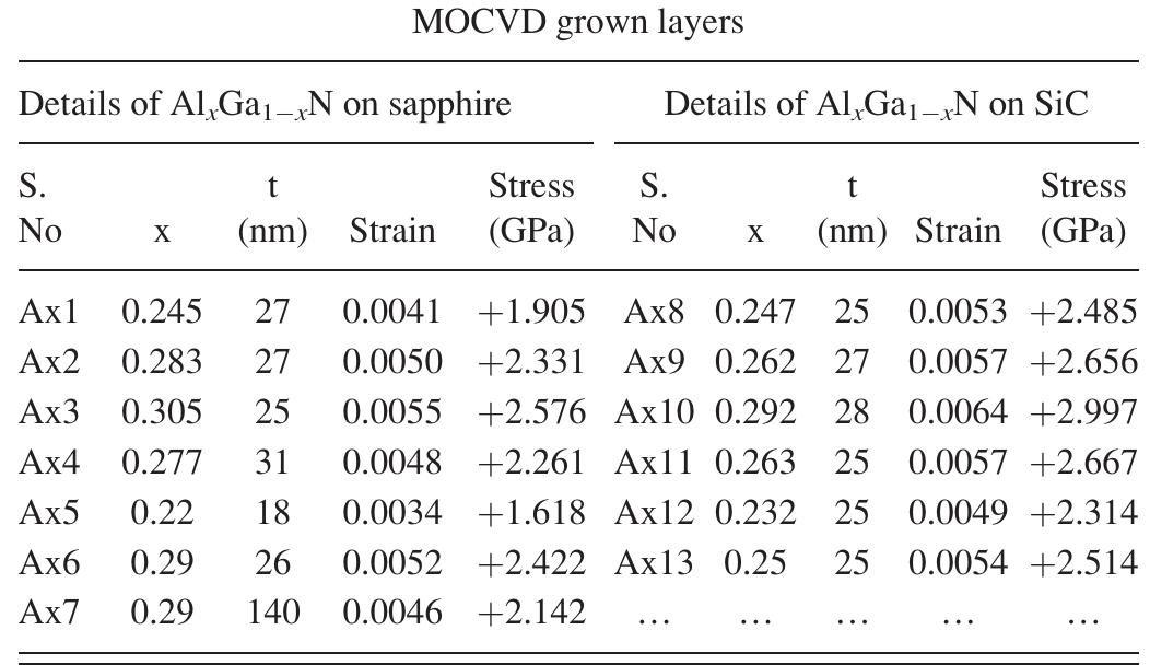
TABLE I. Details of the samples. WELG Lalit UU Usllig TLMindlylital “gapeit bivg ildateiial research diffractometer fitted with a 2-D detector and Ge (220) four bounce crystals. The diffractometer was equipped using CuK«1 source with multiple crystals in both the inci- dent and diffracted arms and has a resolution of 12 arc sec. The coupled (20-m) scans were recorded for symmetric (00.4) and asymmetric (10.5) planes to measure the lattice constants. The values of lattice parameters a and c were then calculated from the measured peak positions of symmetric and asymmetric reflections, respectively. The composition and thickness of the Al,Ga,_,N epitaxial layers were deter- mined from the simulation of the x-ray diffraction data using the x’pert epitaxy software and is given in Table I. The standard deviation of composition and thickness values were +0.001 and +1 nm, respectively. The thickness variation of Al,.Ga,_,N across the wafer was also determined on a typical wafer and was found to be <2nm. The PL and Raman meas- urements were carried out in a Horiba HR Evolution confo- cal micro-Raman spectrometer equipped with a 40x UV objective, 2400 grooves per mm grating, and a UV enhanced Peltier cooled CCD detector. 4th harmonic solid state Nd:YAG laser with a lasing wavelength of 266 nm was used for excitation. A Gatan mono CL?** cathodoluminescence (CL) system fitted on a Gemini column of Zeiss SUPRA 55 FESEM was used for spectroscopic CL measurements. A Peltier cooled high efficiency PMT detector was used for monochromatic CL measurements. The surface roughness was measured on these samples using Agilent LS 5600 AFM.
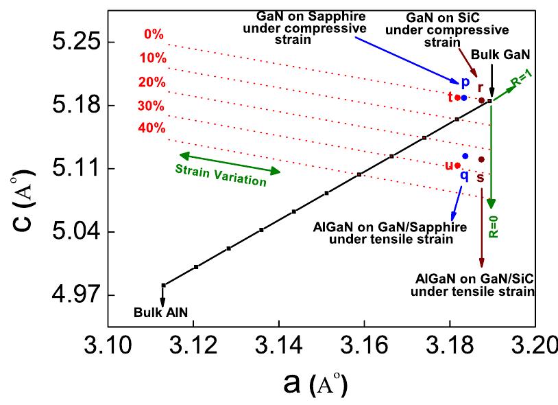
FIG. 1. Plot of "c" versus "a" for various values of AlGaN composition and the dotted lines are iso-composition lines. The points r, p, t represent the measured value of a and c for GaN and s, q, u for the AlGaN layers for the three samples Ax1, Ax8, and Ax7, respectively. Using this equation with known values of co, a, and D, straight lines with a slope —Dco/ap can be drawn to represent iso-composition line between a fully relaxed and fully strained lattice point (shown as dotted lines in Fig. 1). Each point on the iso-composition line would represent a distinc- tive value of c and a depending on the stress state of the layer. A shift towards the left from relaxed value indicates compression and to the right shows that the layer is tensile in nature. The values of lattice constants a and c for GaN on sapphire and SiC substrates for two representative samples Ax! and Ax8 were determined by HRXRD and are shown as points p and r, respectively, in Fig. 1. Corresponding values for the pseudomorphic Al,Ga,;_,N layers on GaN for the same samples are shown as points q and s, respectively. The GaN layers grown on sapphire are more compressive than on
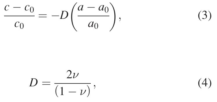
c and a are the measured values in the strained layer, co and ap are the values for relaxed layers, and v is Poisson’s ratio of Al,Ga,_,N, which is a function of composition obtained from the linear interpolation between GaN and AIN binary values. Equation (3) can be re-written as of GaN and AIN, respectively. '* The relaxed values of lattice constants aj and cg for various arbitrary composition of Al,Ga,_,N are obtained by Vegard’s law (Eqs. (1) and (2)) and are shown by bold straight line in Fig. 1. In biaxially strained alloy film, the in-plane and out of plane lattice param- eters are both affected by composition and strain. One sym- metric and one asymmetric reflections are needed to calculate the in-plane and out of plane lattice parameters.'*!° For biax- ial strained hexagonal systems, the out-of-plane strain is related to the in-plane strain by the distortion factor pe
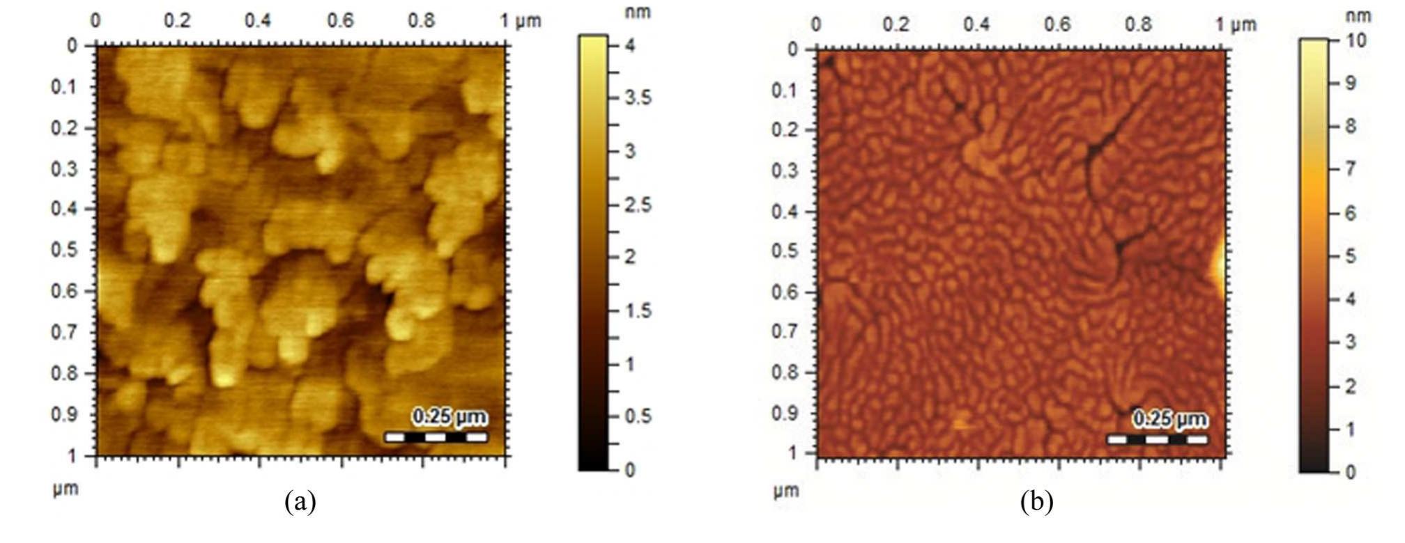
FIG. 2. 1 wm x 1 wm AFM images of samples (a) Ax1, (b) Ax8. surface morphology in sample Ax8 (Fig. 2(b)) is perhaps due to coalescence boundaries. Further, we have examined other samples in this composition range which show similar mor- phology. Surface roughness on Axl and Ax8 was measured as 0.56 and 0.62 nm, respectively. SiC, since point p is more towards the left. The value of strain €,, was then determined from the following equation:
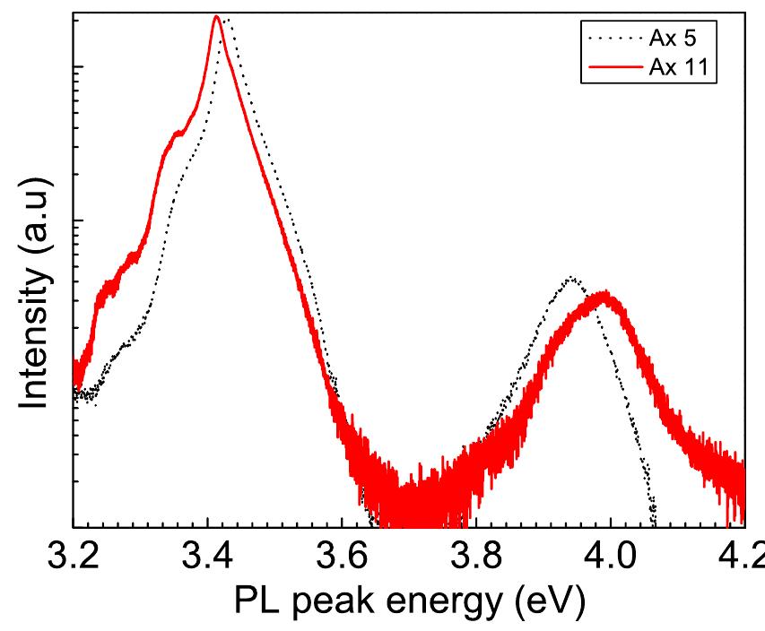
FIG. 3. PL Intensity as a function of energy (...) for Ax5 and (——) fo Axl11. The PL measurements were carried out on all the sam- ples at room temperature and a typical PL spectra of samples Ax5 and Ax11 grown on sapphire and SiC, respectively, are shown in Fig. 3. The GaN PL peak position in Ax5 grown on sapphire is at higher energy, whereas the PL peak position
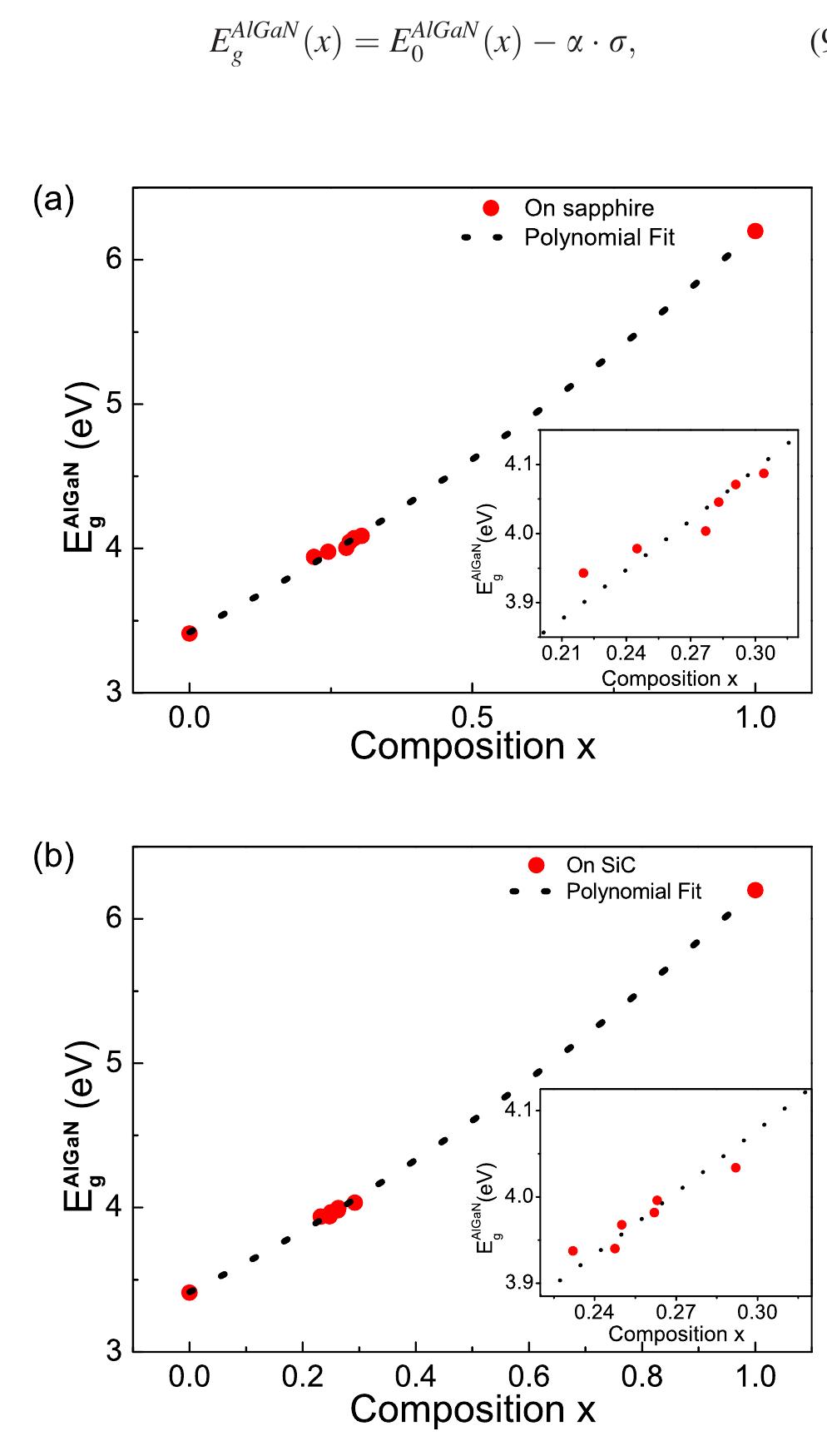
FIG. 4. The measured values of PL peak energy Egan as a function of com. position for Al,Ga;_,.N grown on (a) GaN/sapphire and (b) GaN/SiC. Inse shows the magnified view of the region of interest. for the sample Axl! grown on silicon carbide is at lower energy and the difference in PL peak position between the two samples is about 15 meV. This is due to the difference in the value of compressive stress in GaN grown on sapphire and silicon carbide as mentioned earlier. However, Al,.Ga,_,N peak position difference is due to the combined effect of composition and biaxial tensile strain in the layer. The measured values of PL peak energy Bacay as a function of composition for Al.Ga;_,N grown on GaN/sapphire and GaN/SiC are shown in Fig. 4. The bowing parameters from the polynomial fit to the data were 0.76+ 0.05 and 0.82 = 0.03 eV, respectively, for layers grown on sapphire and SiC. The bowing value obtained from a direct fit of measured PL peak energy position may not be correct as it does not take into account the effect of residual stress in the Al,.Ga,_,N and GaN layers. As pointed out earlier, there is a wide variation of bowing parameter’? in the existing litera- ture as the correct estimation of bowing should involve the inclusion of stress in the band gap evaluation. The value of energy band gap corrected for stress is given by the follow- ing equation:
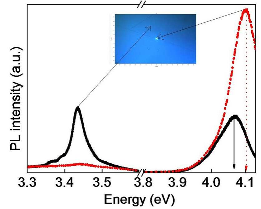
FIG. 5. PL spectra of Ax7 sample at crack (...) and away from crack (——) Inset shows the optical image of the sampled area.
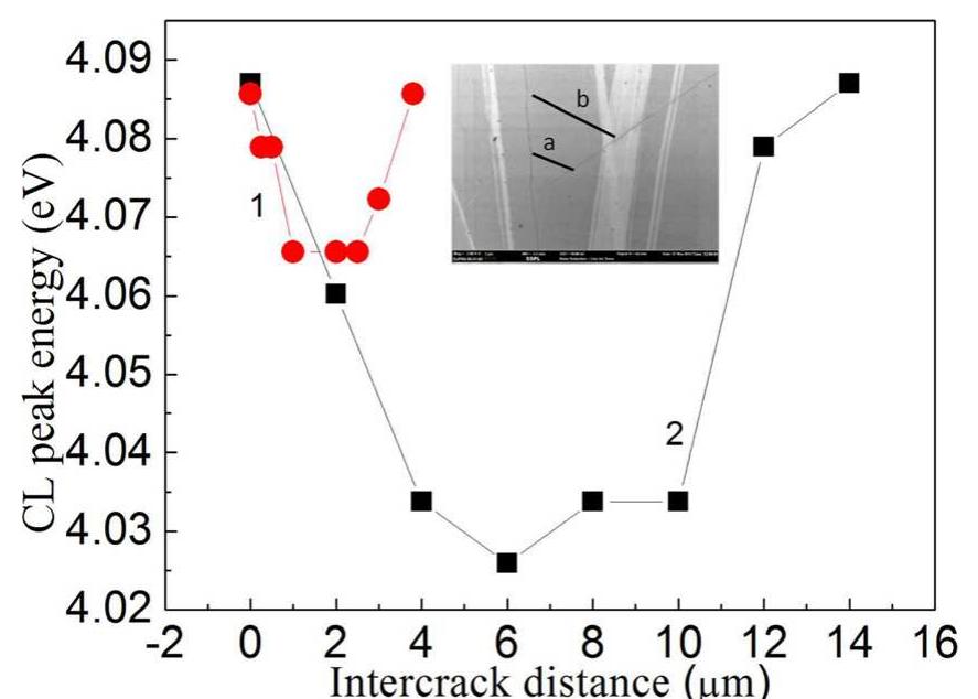
FIG. 6. CL peak energy as a function of distance from crack. Curve | (@) is for intercrack-distance of 4 um (line a) and curve 2 (Mi) is for inter-crack dis- tance of 14 wm (line b). Inset shows the FESEM image of surface with cracks.
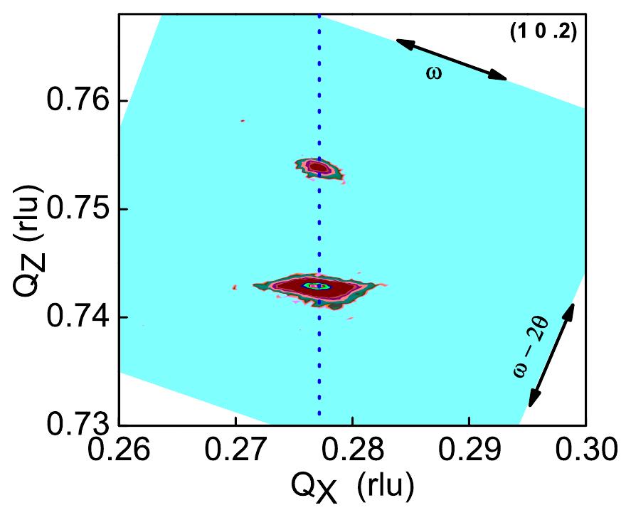
AAYEL IS UNO WHSUe sulss., Lills ValidttOll OF Ul, Ped CHUlsy and subsequent strain with inter-crack distance was also reported by Einfeldt er al.”* in which they have shown that if the crack separation is large, the strain reliefs due to the for- mation of crack are negligible in the middle portion as com- pared to the region near the cracks. In the present case, CL peak energy measured on the crack was 4.087eV, which would correspond to fully relaxed Al 9Ga7z,N band edge (EAGan (x)) and its value in the middle region (curve2) was 4.033eV equivalent to the strained band edge (eyo ). Thus, CL peak energy of 4.065 eV observed in line | indi- cates partially strained region. The reciprocal space map shown in Fig. 7 indicates that Al,Ga,_,N is indeed strained. The value of stress obtained for Ax7 from the HRXRD measurements was 2.142GPa. Substituting the values of EA/GN (x) and BANGaN (x) in Eq. (9), we obtained a as 25.2 meV/GPa. The value of « was also determined from the GaN PL peak position (dE,(GaN) = 15 meV) and stress dif- ference (do(GaN) = 0.6 GPa) in Ax! and Ax8 and was found to be 25 meV/GPa. Same value of pressure coefficient « for GaN and Alo.29Gao.7,N indicates that « is independent of composition in the range 0<x<0.3. Our value of « is in agreement with that obtained by Shan er al.*! in their pres- sure dependent optical absorption studies.
FIG. 9. Stress corrected band gap as a function of measured PL peak energy for layers grown on sapphire (Ml) and SiC (@) substrates. In order to determine the stress corrected band gap value from the measured PL peak position, the data of corrected band gap E4'°*‘(x) was plotted against the measured PL peak position Eee (x) for six samples each of Al,Ga;_.N layers on sapphire and SiC substrates (Fig. 9). The strain cor- rected band gap values can be read from this figure for each measured PL peak positions for pseudomorphic Al,Ga,_,N/ GaN layers grown on sapphire and SiC substrates. Using these values of corrected band gap, corresponding composi- tion can be obtained directly from Fig. 8. The following empirical relation can be used to determine the composition x in case of pseudomorphic Al,Ga,;_,N/GaN layers grown on sapphire and SiC substrates from measured PL peak position
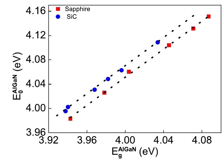
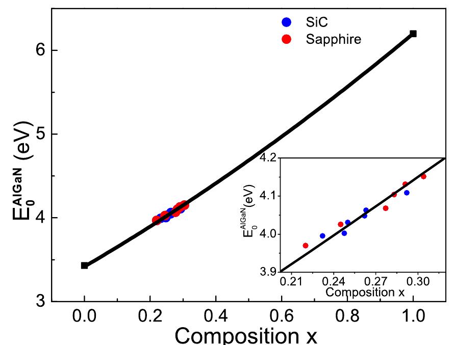
FIG. 8. Stress corrected band gap as a function of Al-composition for pseu- domorphic AlGaN/GaN layers on sapphire and SiC substrate. Inset shows the magnified view of the region of interest.

Loading Preview
Sorry, preview is currently unavailable. You can download the paper by clicking the button above.
References (25)
- U. K. Mishra, P. Parikh, and Y.-F. Wu, Proc. IEEE 90, 1022 (2002).
- M. Beeler, C. Bougerol, E. Bellet-Amalric, and E. Monroy, Appl. Phys. Lett. 103, 091108 (2013).
- M. S. Shur and M. A. Khan, GaN and Related Materials II, edited by S. J. Pearton (Gordon and Breach, Amsterdam, 2000), p. 47.
- H. Sodabanlu, J.-S. Yang, M. Sugiyama, Y. Shimogaki, and Y. Nakano, Appl. Phys. Lett. 95, 161908 (2009).
- E. Monroy, F. Guillot, B. Gayral, E. Bellet-Amalric, D. Jalabert, J.-M. G erard, L. S. Dang, M. Tchernycheva, and F. Julien, J. Appl. Phys. 99, 093513 (2006).
- T. Wethkamp, K. Wilmers, N. Esser, W. Richter, O. Ambacher, H. Angerer, G. Jungk, R. Johnson, and M. Cardona, Thin Solid Films 313, 745 (1998).
- D. Wickenden, C. Bargeron, W. Bryden, J. Miragliotta, and T. Kistenmacher, Appl. Phys. Lett. 65, 2024 (1994).
- L. H. Robins, J. R. Lowney, and D. K. Wickenden, J. Mater. Res. 13, 2480 (1998).
- M. Bremser, W. Perry, T. Zheleva, N. Edwards, O. Nam, N. Parikh, D. Aspnes, and R. F. Davis, MRS Internet J. Nitride Semicond. Res. 1, e8 (1996).
- S. Nikishin, G. Kipshidze, V. Kuryatkov, K. Choi, I. Gherasoiu, L. Grave de Peralta, A. Zubrilov, V. Tretyakov, K. Copeland, T. Prokofyeva et al., J. Vac. Sci. Technol., B 19, 1409 (2001).
- H. Jiang, G. Zhao, H. Ishikawa, T. Egawa, T. Jimbo, and M. Umeno, J. Appl. Phys. 89, 1046 (2001).
- S. Lee, A. Wright, M. Crawford, G. Petersen, J. Han, and R. Biefeld, Appl. Phys. Lett. 74, 3344 (1999).
- P. F. Fewster and N. L. Andrew, J. Appl. Crystallogr. 28, 451 (1995).
- H. Angerer, D. Brunner, F. Freudenberg, O. Ambacher, M. Stutzmann, R. Hopler, T. Metzger, E. Born, G. Dollinger, A. Bergmaier et al., Appl. Phys. Lett. 71, 1504 (1997).
- M. Moram and M. Vickers, Rep. Prog. Phys. 72, 036502 (2009).
- M. Schuster, P. Gervais, B. Jobst, W. H€ osler, R. Averbeck, H. Riechert, A. Iberl, and R. St€ ommer, J. Phys. D: Appl. Phys. 32, A56 (1999).
- C. Kisielowski, J. Kr€ uger, S. Ruvimov, T. Suski, J. Ager III, E. Jones, Z. Liliental-Weber, M. Rubin, E. Weber, M. Bremser et al., Phys. Rev. B 54, 17745 (1996).
- S. Raghavan and J. Redwing, J. Appl. Phys. 98, 023515 (2005).
- J.-M. Wagner and F. Bechstedt, Phys. Rev. B 66, 115202 (2002).
- S. Choi, E. Heller, D. Dorsey, R. Vetury, and S. Graham, J. Appl. Phys. 113, 093510 (2013).
- W. Shan, J. W. Ager, K. Yu, W. Walukiewicz, E. Haller, M. Martin, W. McKinney, and W. Yang, J. Appl. Phys. 85, 8505 (1999).
- O. Madelung, U. R€ ossler, and W. Von der Osten, Intrinsic Properties of Group IV Elements and III-V, II-VI and I-VII Compounds (Springer, 1987).
- S. Lee, D. Koleske, K. Cross, J. Floro, K. Waldrip, A. Wise, and S. Mahajan, Appl. Phys. Lett. 85, 6164 (2004).
- S. Einfeldt, M. Dießelberg, H. Heinke, D. Hommel, D. Rudloff, J. Christen, and R. Davis, J. Appl. Phys. 92, 118 (2002).
- A. Wright and J. Nelson, Appl. Phys. Lett. 66, 3051 (1995).