Consistent model for short-channel nMOSFET after hard gate oxide breakdown (original) (raw)
Abstract
Dissimilar post-hard-breakdown nMOSFET characteristics are consistently explained by the location of a constant-size breakdown path. Device simulations with the breakdown path modeled as a narrow inclusion of highly doped n-type silicon well reproduce all postbreakdown nFET characteristics, including the substrate current behavior, for both gate-to-substrate and gate-to-extension breakdowns. An equivalent circuit describing the gate current in an nFET after hard gate-oxide breakdown is proposed.
Figures (10)
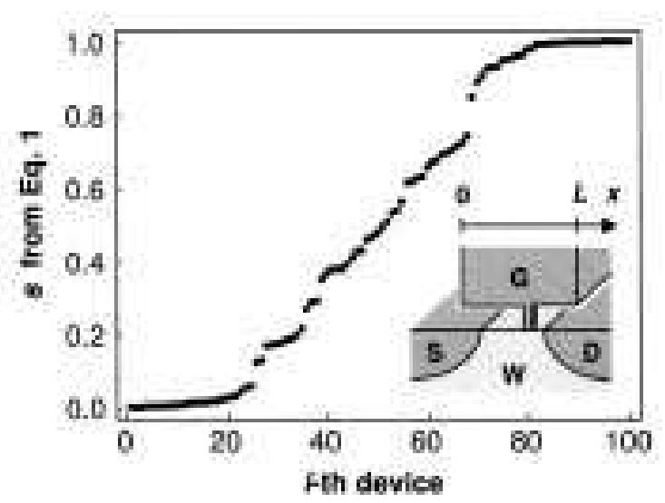
Fig. 1. Sorting s-values (1) measured on n = 100 E = 0.20 jem nFETs at Ve = —1.5 V gives the absolute positions x of the breakdown spots on the respective devices (2), provided the breakdown spots are randomly distributed along the entire gate length L. Inset: FET/breakdown path geometry.
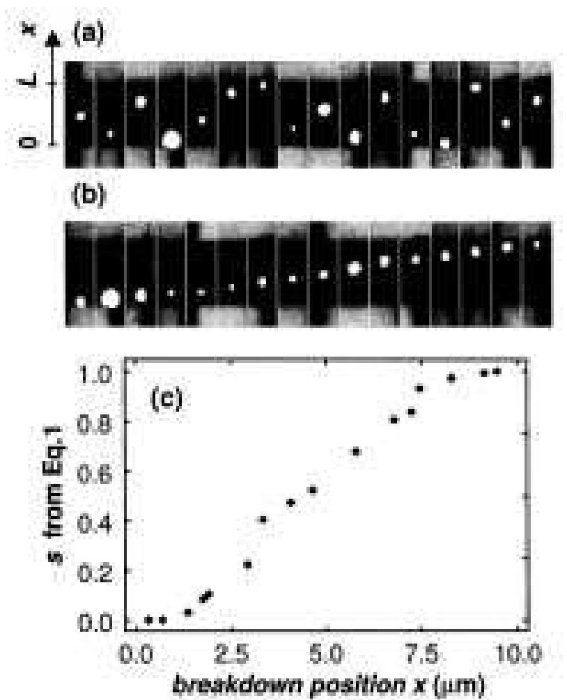
Fig. 2. Emission microscope images of 16 L = 10 ym nFETs after gate-oxide breakdown taken at V;, between 2 and 3 V (a) ordered randomly and (b) sorted according to parameter s determined on each FET. (c) Parameter s is a unique monotonic function of the breakdown spot position x detemined from (a) for each of the 16 FETs. Approximately equidistant spacing between ordered breakdown positions is apparent in (b) and (c).
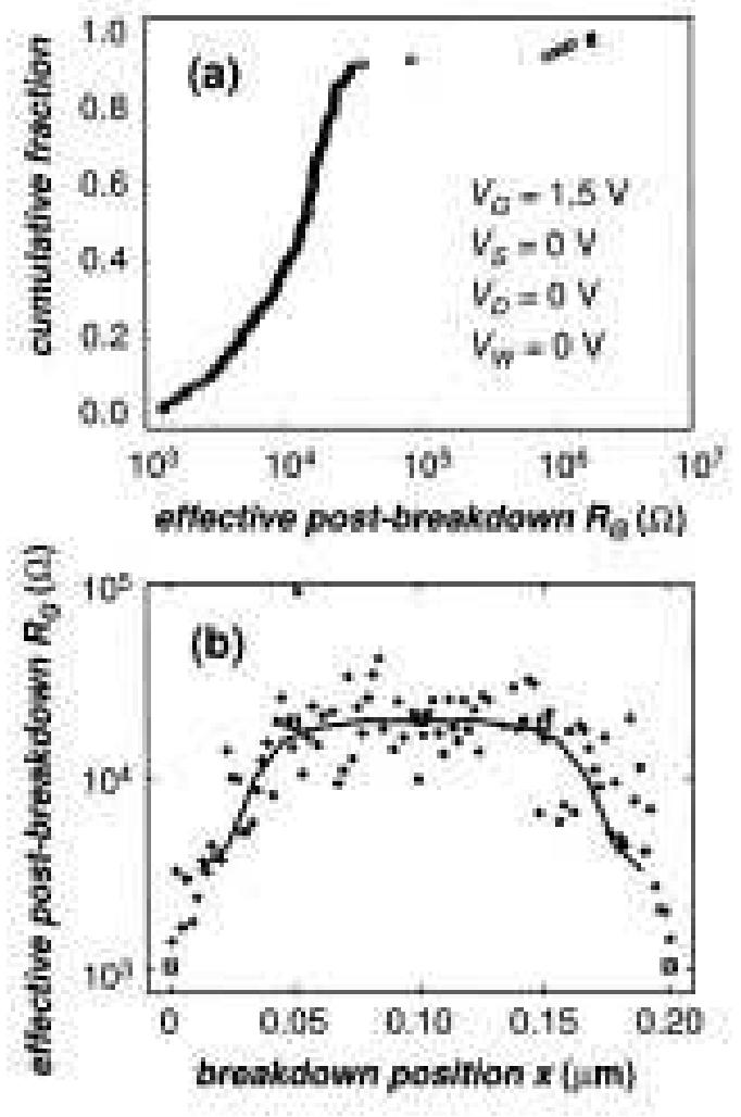
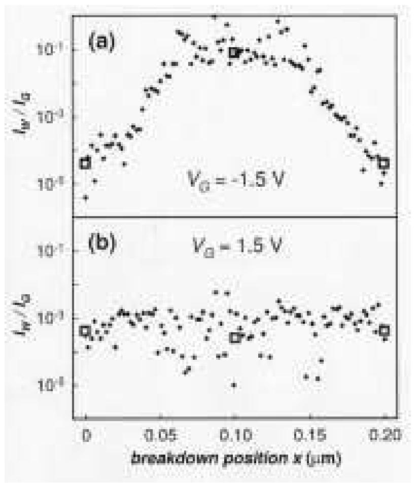
Fig. 3. Effective gate postbreakdown resistance (a) measured on 100 L = 0.20 ym nFETs can be deconvoluted as (b) a function of the breakdown position. R~ increases by a factor of ~ 20 for breakdowns above the FET channel. Both the MEDICI (line) and the SPICE (open squares) calculations using, respectively, the proposed physical model and the equivalent circuits for an nFET after hard gate breakdown fit the distribution well.
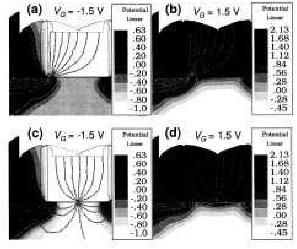
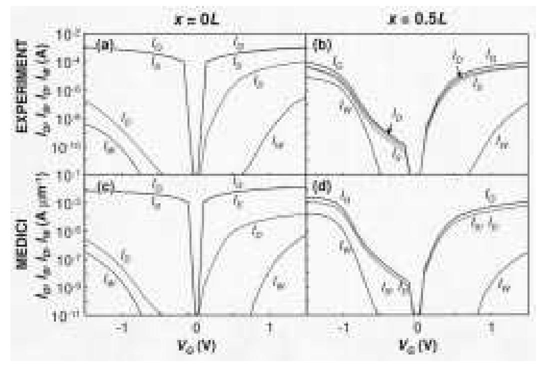
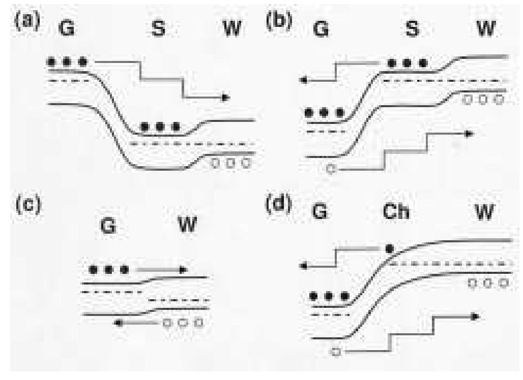
Fig. 5. Potential distributions and current flowlines calculated with MEDICI for gate-to-extension (2 = 0 sm) breakdown at Vg = Vp = Vy = 0 V and (a) V¢ = —1.5 V and (b) Ve = 1.5 V, and for gate-to-substrate (2 = 0.5L) breakdown at (c) Ve = —1.5 V and (d) Ve = 1.5 V. (a)-(b) Electrons are driven through the breakdown path by the electric field across the path. (c) Electrons are emitted from the gate, diffuse through the substrate and are collected at the source and the drain (bipolar effect). (d) Electrons flowing from source and drain in the channel controlled by the gate are pulled through the breakdown path into it (FET effect). Fig. 4. (a)-(e) Postbreakdown measurements on E = 0.20 yxm nFETs with hard breakdown located at the given x. (f)-(j) MEDICI simulation with 5 nm wic breakdown path at the corresponding «. Sublinear behavior of J, in (f) and (j) is ascribed to current crowding in the MEDICI simulation. (k)-(0) SPICE calculatic using the circuits in Fig. 6 with Ryo: fixed at 1 kQ.
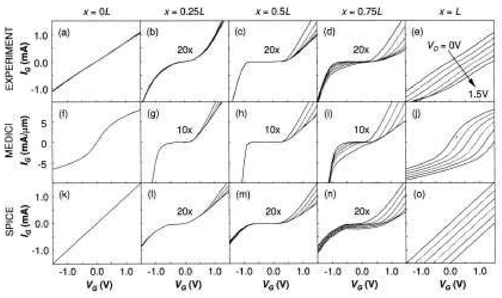
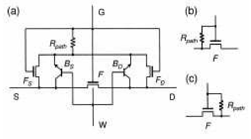
Fig. 6. (a) Equivalent circuit for an nFET with gate-to-channel breakdown. F represents the unbroken nFET. This circuit collapses (b) for 2 — 0 jm to the gate-to-source extension breakdown and (c) fora — L to the gate-to-drain extension breakdown.
AN ve Neersgiecer received We M.o, Gegree if physics from the University of Gent, Belgium, in 1984. She joined IMEC in 1985, working on process modeling. She has been involved in modeling and simulation work for several European projects such as STORM (implantation and diffusion modeling in silicon, diffusion in silicides), ADEQUAT, ACE, and HUNT (process and device simulation for CMOS). At present she is mainly focussing on process and device simulation and calibration of 0.13um and smaller CMOS technologies. Next to this she is also esponsible for support of TCAD tools used at IMEC.

Loading Preview
Sorry, preview is currently unavailable. You can download the paper by clicking the button above.
References (20)
- K. Okada, H. Kubo, A. Ishinaga, and K. Yoneda, "A concept of gate oxide lifetime limited by 'B-mode' stress induced leakage currents in direct tunneling regime," Symp. VLSI Technol. Dig., pp. 57-58, 1999.
- B. Kaczer et al., "Impact of MOSFET oxide breakdown on digital circuit operation and reliability," in IEDM Tech. Dig, 2000, pp. 553-556.
- B. Kaczer, R. Degraeve, M. Rasras, K. Van de Mieroop, P. J. Roussel, and G. Groeseneken, "Impact of MOSFET gate oxide breakdown on digital circuit operation and reliability," IEEE Trans. Electron Devices, vol. 49, pp. 500-506, Mar., 2002.
- T. Pompl, H. Wurzer, M. Kerber, R. C. W. Wilkins, and I. Eisele, "Influ- ence of soft breakdown on NMOSFET device characteristics," in Proc. IRPS, 1999, pp. 82-87.
- R. Degraeve, B. Kaczer, A. De Keersgieter, and G. Groeseneken, "Rela- tion between breakdown mode and breakdown location in short channel nMOSFET's and its impact on reliability specifications," in Proc. IRPS, 2001, pp. 360-366.
- B. Kaczer, R. Degraeve, A. De Keersgieter, K. Van de Mieroop, T. Bearda, and G. Groeseneken, "Consistent model for short-channel nMOSFET post-hard-breakdown characteristics," in Symp. VLSI Technol., 2001, pp. 121-122.
- M. Rasras, I. De Wolf, G. Groeseneken, R. Degraeve, and H. E. Maes, "Substrate hole current origin after oxide breakdown," in IEDM Tech. Dig., 2000, pp. 537-540.
- F. Crupi et al., "Characterization of soft breakdown in thin oxide nMOSFET's based on the analysis of the substrate current," IEEE Trans. Electron Devices, vol. 48, pp. 1109-1113, June 2001.
- N. Yang, W. K. Henson, and J. J. Wortman, "Analysis of tunneling currents and reliability of nMOSFET's with sub-2 nm gate oxides," in IEDM Tech. Dig., 1999, pp. 453-456.
- B. P. Linder et al., "Gate oxide breakdown under current limited constant voltage stress," in Symp. VLSI Technol. Dig., 2000, pp. 214-215.
- P. Roussel, R. Degraeve, G. Van den bosch, B. Kaczer, and G. Groe- seneken, "Accurate and robust noise-based trigger algorithm for soft breakdown detection in ultra thin oxides," in Proc. IRPS, 2001, pp. 386-392.
- E. Wu, E. Nowak, J. Aitken, W. Abadeer, L. K. Han, and S. Lo, "Struc- tural dependence of dielectric breakdown in ultra-thin gate oxides and its relationship to soft breakdown modes and device failure," in IEDM Tech. Dig., 1998, pp. 187-190.
- H. Satake and A. Toriumi, "SiO dielectric breakdown mechanism studied by the post-breakdown resistance statistics," Semicond. Sci. Technol., vol. 15, pp. 471-477, 2000.
- B. Kaczer, R. Degraeve, A. De Keersgieter, M. Rasras, and G. Groe- seneken, "Explanation of nMOSFET substrate current after hard gate oxide breakdown," Microelectron. Eng., vol. 59, pp. 155-160, 2001.
- S. Ikeda, M. Okihara, H. Uchida, and N. Hirashita, "Cross-sectional transmission electron microscope studies on intrinsic breakdown spots of thin gate oxides," Jpn. J. Appl. Phys., vol. 36, p. 2561, 1997.
- M.-Y. Tsai, H.-C. Lin, D.-Y. Lee, and T.-Y. Huang, "Post-soft-break- down characteristics of deep submicron nMOSFET's with ultrathin gate oxide," IEEE Electron Device Lett., vol. 22, pp. 348-350, July 2001.
- T.-S. Yeoh, N. R. Kamat, R. S. Nair, and S.-J. Hu, "Gate oxide break- down model in MOS transistors," in Proc. IRPS, 1995, pp. 149-155.
- T. Ghani et al., "100 nm gate length high performance/low power CMOS transistor structure," in IEDM Tech. Dig., 1999, pp. 415-418.
- S.-I. Takagi and M. Takayanagi, "Carrier transport properties of thin gate oxides after soft and hard breakdown," Microelectron. Eng., vol. 59, pp. 5-15, 2001.
- M. Rasras, I. De Wolf, G. Groeseneken, R. Degraeve, and H. E. Maes, "Substrate hole current origin after oxide breakdown," J. Appl. Phys., to be published. Ben Kaczer received the M. S. degree in physical electronics from Charles University, Prague, Czech Republic, in 1992, and the M. S. and Ph. D. degrees in physics from The Ohio State University in 1996 and 1998, respectively. For his Ph.D. research on the ballistic-electron emission microscopy of SiO and SiC films, he received an OSU Presidential Fellow- ship and a financial support from Texas Instruments, Inc. In 1998, he joined the Technology Reliability and Yield group of IMEC, where his activities include the research of the degradation phenomena and the reli- ability prediction of SiO , high-k, and ferroelectric films.