A new anticounterfeiting marking system (original) (raw)
2011, Nanotec IT Newsletter 12, 19-21 (2011)
Abstract
Counterfeiting is a global problem that can have major social and economic consequences. The spread, number and kind of counterfeit goods has greatly increased in recent years: according to the study of Counterfeiting Intelligence Bureau (CIB) of the International Chamber of Commerce (ICC), counterfeit Goods make up 5 to 7% of World Trade. In a recent update OECD has estimated in $250 billion in 2007 the worldwide value of international trade in counterfeit and pirated goods. As a consequence, there is a urge in developing and adopting innovative anti-counterfeiting technologies able to ensure a real protection and/or traceability of a number of items, including, e.g., forensic documents, dan-gerous waste, strategic components (like microprocessors in automo-tive/aerospace fields, both civilian and military), pharmaceutical products, currency notes, identity/credit/debit cards, quality control, commercial/artistic objects. Our Laboratory in ENEA has recently developed a new method to fight counterfeiting and to trace critical goods, based on our know-how in the fields of optics, laser, plasma and radiation-matter interaction. Our technology allows to vary the protection level in relation to the desired extent by properly increasing the complexity of the marking procedure. On the other side, the specific reading technique is straightforward using a dedicated apparatus.
Figures (30)

EXPLOITING NATURAL SELF ASSEMBLY to IMPROVE DETECTION SENSITIVITY Figure 1. The ANANAS concept vs monomerica avidin.

Figure 2 ANANAS (0) vs commercial avidin-HRP (¢) in a model ELISA assay. Arrows indicate the positive signal onsets (signal/stdv >2). than 0.023 pg/well. In the same analytical set-up, the positive si- gnal onset for the commercial competitor avidin-HRP was at 6.17 pg/well. The ANANAS enhanced sensitivity is due to both lower noise and higher signal intensities. The enhancement factor in this analytical set-up (calculated from the ratio of the two onset values) was of about 240 fold.

Figure 4 shows preliminary data obtained in a real analytical con- text, namely in the detection of anti-BHV1 (Bovine herpes virus type 1) IgGs in cow milk. The presence of these antibodies in milk is due to either infection or immunization with BHV1. Figure 4. Detection of anti-BHV1 IgGs in six positive cow milk samples, each diluted with negative milk. The dilutions tested are 1 to 10; 1 to 20, 1 to 50 and 1 to 125

Figure 3. Detection of mouse IgGs from serum in a dot blot experiment using the ANANAS system and commercial enhanced Vectatstain ABC system. Spots (1l) were made with mouse serum serially diluted from 1:10000 to 1:640000 in PBS/BSA. Figure 3 shows the analytical performance of the ANANAS sy- stem in a blot assay where the analyte was mouse IgG from se- rum, which was diluted serially into PBS/BSA. In this case, the ANANAS performance was compared to that of the commercial competitor Vectastain ABC from Vector Labs, which relies on a patented avidin-based amplifying technology. The results of this assay can be used to predict the efficacy of detection in Western or Southern blots.

Fig. 2 Screenshot of the NanoPlan therapy planning software Fig 1: The NanoTherm magnetic fluid The next component of the NanoTherm therapy is the NanoPlan therapy software, which supports the treating physician in the de- velopment of a treatment planning. Based on the distribution of the nanoparticles as shown in a post-operative CT scan, NanoPlan uses the Bioheat-Transfer equation to estimate the treatment


![Figure 2 Output of a random laser made by grinding a laser crystal into a powder and exciting it optically. The random series of lines is due to the speckle generated by the random structure and corresponds to the modes of the random laser. [From: Stefano Gottardo, Riccardo Sapienza, Pedro D. Garcia, Alvaro Blanco, Diederik S. Wiersma, and Cefe Lopez, Resonance-driven random lasing, Nature Photonics 2, 429 (2008).] Even though the same spheres with the same single scattering properties are used, their cumulative behaviour after assembly will depend heavily on the way the spheres as packed together. This is due to the interference between the scattered waves and the way the waves are multiply scattered from one sphere to another. If the spheres are packed according to a crystal-like structure then the interference will be constructive only in cer- tain well defined directions, giving rise to Bragg refraction and reflection. In the disordered case the light waves will perform a random walk from one sphere to the other. The occurrence of interference effects is now less obvious to understand, however also in random systems interference effects turn out to be very important [1].](https://figures.academia-assets.com/32084957/figure_008.jpg) ](
](Figure 2 Output of a random laser made by grinding a laser crystal into a powder and exciting it optically. The random series of lines is due to the speckle generated by the random structure and corresponds to the modes of the random laser. [From: Stefano Gottardo, Riccardo Sapienza, Pedro D. Garcia, Alvaro Blanco, Diederik S. Wiersma, and Cefe Lopez, Resonance-driven random lasing, Nature Photonics 2, 429 (2008).] Even though the same spheres with the same single scattering properties are used, their cumulative behaviour after assembly will depend heavily on the way the spheres as packed together. This is due to the interference between the scattered waves and the way the waves are multiply scattered from one sphere to another. If the spheres are packed according to a crystal-like structure then the interference will be constructive only in cer- tain well defined directions, giving rise to Bragg refraction and reflection. In the disordered case the light waves will perform a random walk from one sphere to the other. The occurrence of interference effects is now less obvious to understand, however also in random systems interference effects turn out to be very important [1].
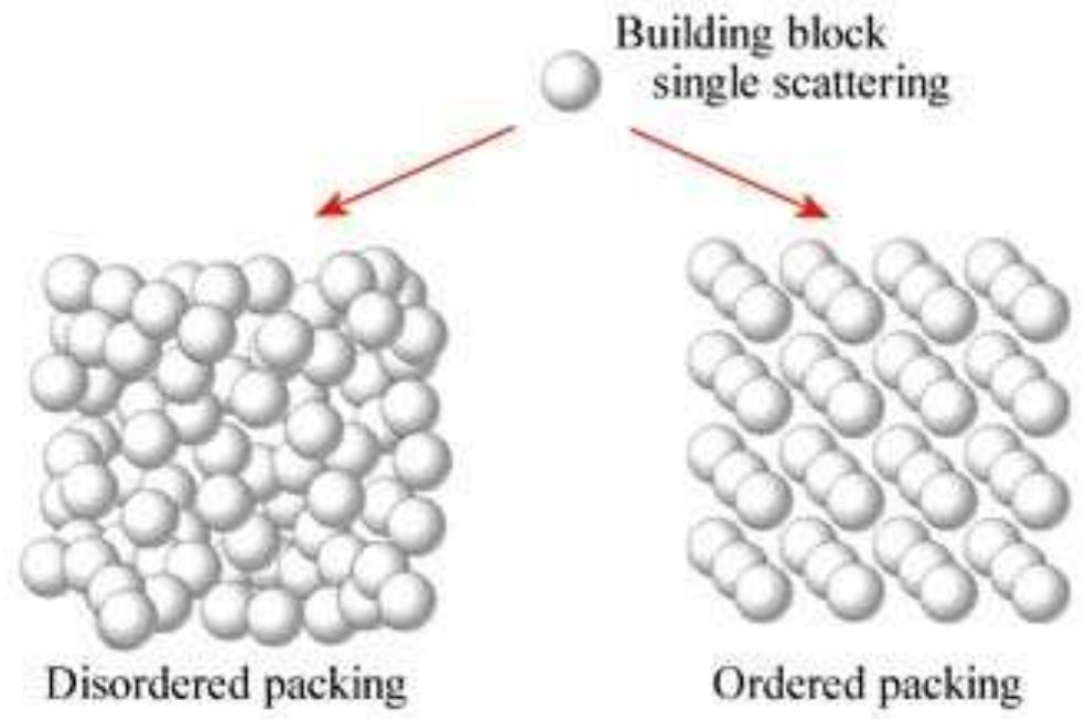
Figure 1 Micro assembly of a complex photonic system. The two extremes are fully disordered assembly (left) leading to random multiple light scattering and ordered assembly (right) resulting in a photonic crystal or possibly a photonic band gap material. I he transport of light in complex dielectric materials is a rich and fascinating topic of research. With complex dielectrics we intend dielectric structures with an index of refraction that has variations on a length scales that is very roughly comparable to the wavelength. Such structures strongly scatter light. A possible building block for constructing a complex dielectric is a micro sphere of diameter comparable to the wavelength and of a cer- tain refractive index that is different from its surrounding me- dium. The single scattering from such a sphere has a rich struc- ture due to internal resonances in the sphere, but its behaviour is well-understood and can be calculated using the formalism of Mie-scattering. A complex dielectric material can then be realized by micro-assembly of several micro spheres. The spheres can be assembled in various ways with as two opposite possibilities a completely disordered packing and a fully ordered assembly. (See Fig.1.)
![Figure 3 Spatial distribution of the light inside a random sample. In a regular disordered structure the distribution is dominated by speckle (left) while in the case of Anderson localization the light is highly localized in space and hence trapped in random modes (right). [From: D.S. Wiersma, P. Bartolini, A. Lagendijk, and R. Righini, Localization of Light in a disordered medium, Nature 390, 671 (1997).] n very strongly scattering materials interference effects can lead to a strong version of localization, also called Anderson locali- zation, being the optical counterpart of localization of electrons n strongly disordered conductors. Anderson localization inhibits the free propagation of waves and the optical diffusion process thereby comes practically to a halt. Although the detailed mecha- nism behind localization is quite complex, one can visualize the effect as being due to the formation of randomly shaped but clo- sed modes with an overall exponentially decaying amplitude. (See Figure 3.) The average spatial extend of these localized modes de- fines a length scale called the localization length. The connection between weak and strong localization is then also immediately clear. While in the case of weak localization the interference oc- curs outside the sample between light waves that have travelled along half-closed loops, in strong localization the same interfe- rence occurs inside the sample along closed-loop paths [2].](https://figures.academia-assets.com/32084957/figure_010.jpg) ](
](Figure 3 Spatial distribution of the light inside a random sample. In a regular disordered structure the distribution is dominated by speckle (left) while in the case of Anderson localization the light is highly localized in space and hence trapped in random modes (right). [From: D.S. Wiersma, P. Bartolini, A. Lagendijk, and R. Righini, Localization of Light in a disordered medium, Nature 390, 671 (1997).] n very strongly scattering materials interference effects can lead to a strong version of localization, also called Anderson locali- zation, being the optical counterpart of localization of electrons n strongly disordered conductors. Anderson localization inhibits the free propagation of waves and the optical diffusion process thereby comes practically to a halt. Although the detailed mecha- nism behind localization is quite complex, one can visualize the effect as being due to the formation of randomly shaped but clo- sed modes with an overall exponentially decaying amplitude. (See Figure 3.) The average spatial extend of these localized modes de- fines a length scale called the localization length. The connection between weak and strong localization is then also immediately clear. While in the case of weak localization the interference oc- curs outside the sample between light waves that have travelled along half-closed loops, in strong localization the same interfe- rence occurs inside the sample along closed-loop paths [2].
![Figure 4 Flights of fancy: an inhomogeneous disordered photonic material can be used to create optical Lévy flights. This new material is also termed Lévy glass and behaves as a superdiffuser for light. [From: Pierre Barthelemy, Jacopo Bertolotti, and Diederik S. Wiersma, A Lévy flight for light, Nature 453, 427 (2008).] In our understanding of transport processes we usually assume that the distance covered at every step of the random walker is not varying very much. This simplification seems reasonable at first sight, since it allows to consider only the average value of this step length, the so called mean free path. Physicists use this simplification, which is based on the central limit theorem, very often. In a Lévy flight the step length of the random walk is far from constant and this means that in some occasions very large steps can occur. These large steps not only mean that the random walker can cover a much vaster area, but they also lead to the counter-intuitive property that the average step length diverges [5-7].](https://figures.academia-assets.com/32084957/figure_011.jpg) ](
](Figure 4 Flights of fancy: an inhomogeneous disordered photonic material can be used to create optical Lévy flights. This new material is also termed Lévy glass and behaves as a superdiffuser for light. [From: Pierre Barthelemy, Jacopo Bertolotti, and Diederik S. Wiersma, A Lévy flight for light, Nature 453, 427 (2008).] In our understanding of transport processes we usually assume that the distance covered at every step of the random walker is not varying very much. This simplification seems reasonable at first sight, since it allows to consider only the average value of this step length, the so called mean free path. Physicists use this simplification, which is based on the central limit theorem, very often. In a Lévy flight the step length of the random walk is far from constant and this means that in some occasions very large steps can occur. These large steps not only mean that the random walker can cover a much vaster area, but they also lead to the counter-intuitive property that the average step length diverges [5-7].

Fig. 3 HRTEM image of TiO, sample. The substitution of graphite, commonly used as anodic material, with oxides at higher voltage, makes the complete cell more sta- ble and therefore more safe, but with lower voltage. The use of a template assisted synthesis makes possible to obtain nanostruc- tured particles also in the case of anodic materials. In particular here is presented a TiO, sample whose particles size is lower of 10 nm, (Fig.3). TiO, particles are very well crystallized.

Fig. 4 Charge—discharge cycling test of TiO, sample at different C-rate (from C/2 to 10) Electrochemical experiments on the complete cell are still running Preliminary data of charge and discharge of one of the prepared samples show a good cyclability of TiO, (Fig.4). The specific capa- city is not far from the theoretical one. The studied sample shows an important loss of capacity after the first cycles, but after these, the electrochemical performance are promising as there is a very slow fading during cycling even at higher C rates. Clara rh aerial Aviation An thaw SARA ete! Amat! A lawn

Fig.2 Charge—discharge cycling test of LiFePO,/C sample at different C-rate (from C/20 to 20C) EC/DEC mixture. This C layer is thick enough to assure a good electronic conduc- tivity, but it is also permeable to Lit ions, to assure the ionic con- ductivity. Cathodic particles are nanostructured: its average size is about 40 nm. These two characteristics, nanosize and carbon coating, permits the complete charge and discharge of the active material contained in the sample.

Fig.1 HRTEM image of LiFePO,/C composite

Fig. 5 HRTEM image of Fe,0, sample. Fe,O, was also synthesized ad it is an interesting material to be used as anode for Liion cells. It is a very low cost and highly en- vironmental friendly materials. Moreover its theoretical capacity is higher than 1000 mAhg", making it very attractive for the au- tomotive application. The TEM micrograph (Fig. 5) shows a well crystallized, nanosized and ordered sample. Nevertheless, though the structural characteristics are very inte- resting by the nanotechnological viewpoint, the electrochemical performance are quite unsatisfying, as shown in Fig. 6. The electrochemical activity falls after few cycles.

Fig. 6 Charge—discharge cycling test of Fe,O, sample at different C-rate (from C/2( to 1C)

Figure 3: — Prototype of the portable reading device able to read the invisible images. On the PC screen there is the coded data matrix (a 2-D binary array) read by the ENEA device on the film, and below, the corresponding sign “WATERMARKING" as decoded by a specific software. A prototype of a portable device able to read the invisible marks is shown in figure 3. In this case an encoding technique has been applied to crypt the hidden pattern. The PC screen shows the raw data matrix (an array of tiny squares as a 2-D barcodes) written on the film as read by the device, and the corresponding pattern “WATER MARKING” decoded by a dedicated software.

Figure 2 — a) Picture taken under natural light illumination of a standard badge (85 mmx54 mm) with an invisible mark within the dashed area; b) Picture taken at the optical microscope (magnification 2.5x) showing the same dashed area a: in a), but using the ENEA reading system. In another prototype, we deposited a thin film of luminescent material on a plastic badge commonly used for credit or identity cards. We exposed the film to ionizing radiation trough a contact mask, thus transferring an invisible image on it, and then we put a standard plastic-coating to protect the badge. Figure 2 shows a comparison between the picture of the badge taken under na- tural light illumination and the image observed using the specific reading system in conjunction with an optical microscope at low magnification (2.5x). It is evident that the pattern becomes visible only in the second case.

Figure 1:— Luminescent pattern obtained by contact lithography and observed at an optical microscope by visible light (a) and by using the ENEA reading technique (b). patented reading technique. The mask pattern is visible only with the appropriate reading system.

Figure 1 Coating of textiles with a CNT containing formulation: if aggregation of CNT occurs, this becomes visible as micrometer-sized dark spots (up): if well- dispersed these spots are prevented and via SEM analysis the individual CNTs car be seen (down).

Figure 2 Coating of textiles with sol gel can improve the abrasion resistance as can be seen by comparing the result of Martindale Testing (EN 18012947 - part 2) after 100.000 cycles on an untreated (left) and treated (right) woven PES substrate. In this case, a thin SiO.- layer is applied on the textile via the sol gel method. This method stems originally from deposition on ce- ramic substrates but by modifying the chemistry, systems which can be cured at temperatures compatible with the most common polymers could be developed.

Figure 1: CNT/Nylon composite fiber, in the inset the I/V curve A specific research line deals with the production and functional characterizations of fibres coated by metallic nanoparticles for biosensing based on plasmonic processes, or textiles containing magnetic nanowires (Figure 3) which can find useful applications for the realizations of advanced textile sensorial systems.

Figure 3: Magnetic nanowires formed by Ni nanoparticles supported on CNT bundles

The results obtained up to now show that the inclusion of nano- structures greatly improve some properties or add new properties to the as-produced textiles. As an example, for textiles impregna- ted with PEDOT/CNT dispersions a surface electrical resistance of about 75 kQ has been measured, and under deformation a resi- stance variation of about 5 kQ/cm has been detected. (Figure 4).

Figure 4: Cotton/CNT textiles prepared by dip-coating: I/V curve and piezo- resistive responses

Info AIRI/Nanotec IT — info@nanotec.it


Partecipazione delle PMI italiane sui diversi temi del programma Cooperation Legenda: SEC — Sicurezza; SPA — Spazio; SSH — Scienze Socio economiche ed Umanistiche; TPT — Trasporti; ENV — Ambente; Energy — Energia; NMP — Nanotecnologie, Materiali, Processi; ICT — Tecnologie per IInformazione e la comunicazione; KBBE — Alimenti, Agricoltura, Pesca e Biotecnologie; Health - Salute go In esame (gen-ott 2U1Q), sempre all interno del Frogramma Cooperation, un incremento della quota di budget indirizzata alle PMI, che raggiunge il 15,4%. Il numero di GA firmati nell’am- bito del tema NMP ha raggiunto, sempre nello stesso periodo, un totale di 329. L'apporto finanziaro per le PMI rappresenta il 23,2% (303MEuro sui 1.305 MEuro), con un contributo medio, per PMI, di 269.405 Euro.

CONANOMET coinvolge 14 organizzazioni nel campo della nano metrologia, nanotecnologie, trasferimento tecnologico e formazione ed @ coordinato da EUSPEN (European Society For Precision Engineering And Nanotechnology www.euspen.eu — Regno Unito). Nel progetto CONANOMET (www.co-nanomet.eu) sono stati definiti i bisogni attuali ed emergenti della nano metrologia, con l‘obiettivo di supportare lo sviluppo e lo sfruttamento economico delle nanotecnologie a sostegno della trasformazione industriale attualmente in corso anche nel nostro Paese. Il progetto, che si é appena concluso, ha affrontato diverse aree connesse alle nano- tecnologie: produzione di nano particelle ingegnerizzate, nano biotecnologie, film sottili, nuove tecniche di indagine nanometri- ca, modellazione e simulazione dei nuovi nanomateriali.

Loading Preview
Sorry, preview is currently unavailable. You can download the paper by clicking the button above.