Parallel In Parallel Out (PIPO) Shift Register (original) (raw)
Last Updated : 24 Apr, 2026
A shift register is an important part of these circuits, which enables sequential data shifting in and out. A PIPO shift register is a collection of flip-flops arranged in a series, with each flip-flop capable of storing one bit of data.
- The primary characteristic that distinguishes a PIPO shift register is its ability to load data and output it in parallel.
- A PIPO shift register loads and outputs all data at once, unlike others that work one bit at a time.
- It stands out for its ability to handle data in parallel, offering significant advantages in certain applications.
- **Shift Register: A digital circuit consisting of flip-flops used to sequentially store and shift data.
- **Flip-Flop: A simple building block of a variable name that can store some data. It can be in the 0 or 1 state.
- **Parallel Input: Input to the PIPO transfer register from the data simultaneously uploaded to the flip-flops. Allows multiple files to be entered simultaneously.
- **Parallel output: Output of the PIPO key register, which can access data stored in the flip-flops. It allows viewing multiple files at the same time.
- **Clock Signal: The time signal is used to synchronize the renaming job. Determines the amount of data that has been changed or replaced in the list.
- **Serial Input: Another input method for converting data to serial input, where data is entered bit by bit sequentially.
- **Serial output: Another output method for extracting data from a switch, where the data is output bit by bit sequentially.
- **Shift Left: A function that shifts data in a scroll to the left. The leftmost bits are discarded, and the new ones are replaced from the right.
- **Shift right: A shift operation where the data in the shift is shifted to the right. Bits on the right are discarded, and new bits are moved to the left.
Working of PIPO Shift Register
Let's discuss an example of a 4-bit shift register to understand the operations of a PIPO shift register. It consists of four flip-flops, labelled D0, D1, D2, and D3. Each flip-flop can store one bit of data. The data can be loaded into the flip-flops simultaneously through the parallel input, known as the Data input. Once the data is loaded, it can be read out simultaneously from each flip-flop through the parallel outputs.
Circuit Diagram
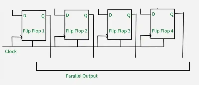
In a PIPO shift register, all flip-flops load and output data simultaneously. There is no shifting of data between flip-flops. This can be accomplished by providing a clock signal that triggers the shifting operation. When the clock signal is activated, the data in each flip-flop is transferred to the adjacent flip-flop, allowing new data to be loaded into the first flip-flop.
**Note: It is important to remember that depending on the shift register's design and specifications, shifting can occur either leftward or rightward.
**Example: Let us Consider,We have a PIPO shift register with four flip-flops (D0, D1, D2, and D3) and parallel inputs (Data). Initially, all flip-flops are cleared and contain the value '0'. We want to load the binary value '**1101' into the shift register using parallel input and then shift the data to the right by two positions.
**Solution:
**Step 1: Parallel Input To load the value '1101' into the shift register, we apply the parallel input as follows:
Data: 1 1 0 1
**Step 2: Clock Cycle (Shift Right) Now, we activate the clock signal to shift the data to the right by two positions. Each clock cycle moves the data in one position to the right. In this case, we perform two clock cycles.
Clock Cycle 1:
Data: 0 1 1 0
Clock Cycle 2:
Data: 0 0 1 1
After two clock cycles, the binary value '1101' has been shifted two positions to the right.
**Step 3: Parallel Output Finally, we can read out the data from the shift register using parallel output. The values stored in the flip-flops after the shifting operation are:
Data: 0 0 1 1
The parallel output provides the binary value '0011', which was obtained after shifting '1101' to the right by two positions. In this above example, we demonstrated the operation of a 4-bit PIPO shift register. we loaded the binary value '1101' in parallel, shifted it to the right by two positions, and obtained the result '0011' through parallel output.
PIPO Shift Register Verilog Code
module PIPO_Shift_Register (
input wire clk, // Clock input
input wire load, // Load signal
input wire [3:0] data_in, // 4-bit input data
output reg [3:0] data_out // 4-bit output data
);
always @(posedge clk) begin
if (load) begin
// Load data into the shift register
data_out <= data_in;
end
end
endmodule
OUTPUT:
- When load is high, then data_out = data_in on the next rising edge of the clock.
- When load is low, then data_out = its previous value.
**Module Declaration: Module PIPO_Shift_Register has inputs as clock clk, load signal load and 4-bit input data data_in with output as the 4-bit data register data_out.
**Always Block: Always @(posedge clk) is a process that occurs on every rising edge of the clock.
The loading of data presented as the 4-bit input into an output register when the load signal is high.
Advantages
- **Flexibility: There is a facility for scalable production without heavy investments in resources.
- **Reduced Capital Investment: There is less need to invest in equipment, tooling, and inventory.
- **Risk Management: Diversifies supply chain as a way of mitigating risk of internal failures.
- **Leverage Supplier Expertise: Components can be of higher quality coming from specialized suppliers.
- **Shorter Lead Times: Using external suppliers can shorten production lead times. Space Optimization: It facilitates more space since pallets can be stacked vertically.
- **High-Speed Data Transfer: Transfer of data takes place at a very high speed, due to parallel input and output.
Disadvantages
- **Higher Pin Count: Due to the nature of inputs and parallel outputs, this requires more pins, adding an additional layer of complexity to the design when compared with serial alternatives.
- **Potential for Signal Skew: Large-scale PIPO systems may experience differences in the time of arrival of signals, reducing the accuracy of the data transfer.
- **Increased Complexity for Large-Scale Designs: Large-scale PIPO shift registers introduce a lot of problems regarding signal integrity and timing, therefore making the design process more cumbersome.
- **Limited Flexibility: Parallel designs may lack the flexibility of serial systems for cases in which applications do not require high-speed parallel processing.
Applications
- **Data storage: PIPO transfer registers are widely used for temporary data storage in digital systems. The parallel upload feature provides fast data entry, while the parallel output allows for on-demand data re-storage.
- **Data Transfer: PIPO shift registers are used in applications where data needs to be transferred from one location to another in a fast manner. By loading the data in parallel and then outputting it simultaneously, PIPO shift registers facilitate high-speed data transmission.
- **Data Manipulation: PIPO shift registers are valuable for performing various data manipulation operations, such as data sorting, arithmetic calculations, and pattern recognition. The ability to process multiple bits of data in parallel enhances the speed and efficiency of these operations.
- **Serial to Parallel Conversion: PIPO conversion can convert serial data to parallel data. This is important when dealing with devices that need to work together. Load data serially and output in parallel, easily switch serial-parallel systems seamless integration.