Intrinsically core-shell plasmonic dielectric nanostructures with ultrahigh refractive index (original) (raw)
A new type of plasmonic nanostructures with topologically protected metallic shells and high–refractive index dielectric cores.
Keywords: Topological insulator, core shell, plasmonics, dielectric, refractive Index
Abstract
Topological insulators are a new class of quantum materials with metallic (edge) surface states and insulating bulk states. They demonstrate a variety of novel electronic and optical properties, which make them highly promising electronic, spintronic, and optoelectronic materials. We report on a novel conic plasmonic nanostructure that is made of bulk-insulating topological insulators and has an intrinsic core-shell formation. The insulating (dielectric) core of the nanocone displays an ultrahigh refractive index of up to 5.5 in the near-infrared frequency range. On the metallic shell, plasmonic response and strong backward light scattering were observed in the visible frequency range. Through integrating the nanocone arrays into a-Si thin film solar cells, up to 15% enhancement of light absorption was predicted in the ultraviolet and visible ranges. With these unique features, the intrinsically core-shell plasmonic nanostructure paves a new way for designing low-loss and high-performance visible to infrared optical devices.
INTRODUCTION
Plasmonic metallic nanostructures have been widely applied in various optical devices, such as optical recording, waveguides, sensors, solar cells, etc. (1, 2). By controlling the geometry and size of metallic nanostructures, electromagnetic waves can be localized and manipulated in nanometer scale. The gold (Au) nanorods facilitate five-dimensional (5D) optical recording based on their excellent wavelength and polarization sensitivity of surface plasmon resonances (3, 4). Silver (Ag) nanoparticles enable electromagnetic energy to be confined and transported below the diffraction limit in plasmonic waveguides, which cannot be realized using conventional waveguides or photonic crystals (5). Au and Ag nanoparticles with plasmon resonances improve the sensitivity of biosensors and push the sensitivity toward the single-molecule detection limit (6). Furthermore, Au, Ag, and aluminum (Al) nanostructures integrated into the absorption layer distinctly enhance the light absorption and energy conversion efficiency in photovoltaic devices (7–9). Plasmonic metallic nanostructures play a key role in the optical devices for realizing new functions and improving the performances. However, metallic nanostructures always demonstrate large parasitic loss in the visible frequency range (10). Such a shortcoming inevitably limits the performance of optical devices.
Alternatively, high–refractive index dielectric nanostructures have been demonstrated as competitive candidates for high-performance optical devices (10, 11). With lower intrinsic loss, they show promise in overcoming the shortcoming of plasmonic metallic nanostructures (12, 13). Moreover, dielectric nanostructures, owing to their intrinsic insulating properties, do not deteriorate the electrical properties of photovoltaic devices. High–refractive index germanium (Ge) nanowires enhance light absorption in photodetectors in intermediate sizes (14). Gradient metasurfaces consisting of dielectric silicon (Si) strip arrays are designed as transparent optical devices to manipulate light, and are capable of achieving ultrathin optical gratings, lenses, and axicons (15). Si nanospheres display controllable electric and magnetic resonances as well as directional light scattering in the visible frequency range, which make them excellent media for light manipulation and harvest in optoelectronic devices (16, 17). In addition, Si slab waveguide achieves optical cloaking that realizes a broadband and low-loss invisibility of objects (18). Nevertheless, compared with plasmonic metallic nanostructures, the light manipulation capability of dielectric nanostructures is inferior at the deep subwavelength scale. Hence, to more effectively manipulate light and achieve high-performance optical devices, it is highly desirable to combine the excellent features of plasmonic metallic nanostructures and dielectric nanostructures in a single nanostructure.
Topological insulators are quantum materials with topologically protected metallic (edge) surface states and insulating (dielectric) bulk states (19). Unique electronic and optical properties, such as the quantum spin Hall effects, exotic Majorana particles, topological magnetoelectric effects, and topological Kerr and Faraday rotation, are expected in topological insulators (20). With these fascinating properties, they hold great potential in developing future electronic, spintronic, and optoelectronic devices. Recently, Dirac plasmon excitations have been observed in binary 3D topological insulator Bi2Se3 micro-ribbon arrays at the terahertz frequency (21). Ultraviolet and visible frequency plasmonics have been observed in the nanoslit arrays and grating of the bulk-insulating quaternary 3D topological insulator Bi1.5Sb0.5Te1.8Se1.2 (BSTS) (22). With an intrinsic metallic surface and an insulating bulk, topological insulators provide an excellent platform for the realization of a new type of nanostructures that could combine the fascinating properties of plasmonic metallic nanostructures and dielectric nanostructures.
Here, we report on the nanofabrication of such a new type of nanostructure, a nanocone, on bulk-insulating topological insulator BSTS single crystals. The fabricated nanocone demonstrates an intrinsically core-shell nanostructure, in which the core is dielectric and the shell is metallic. In contrast to the metallic shell, the dielectric core displays an ultrahigh refractive index of up to 5.5 in the near-infrared frequency range. Plasmonic response and strong backward light scattering were directly observed in the core-shell BSTS nanocone arrays. By integrating the nanocone arrays into an ultrathin amorphous silicon (a-Si) solar cell, 15% enhancements of light absorption in the ultraviolet and visible frequency ranges were achieved.
RESULTS
Bulk-insulating BSTS crystals
For the practical applications of topological insulators in electronic or optical devices, highly insulating bulk states that support conductive surface states are required. However, most discovered topological insulator materials, such as Bi2Se3, Bi2Te3, and Sb2Te3, demonstrate high bulk conductivity due to naturally occurring crystalline defects and the resulting carrier doping (23). On the basis of the experimental observations from angle-resolved photoemission spectroscopy, in these topological insulators, Fermi surface passes through either the bulk conduction band or the bulk valence band, rather than the bulk band gap, which results in a mixture of the surface conductivity with the bulk conductivity (24, 25). To take advantage of the novel electronic properties of topological surface states, bulk defects and conductivity have to be substantially decreased.
Recently, quaternary BSTS has been demonstrated as a desirable topological insulator material with a highly insulating bulk state, and showing surface-dominated electronic transport (26–28). The chemical characteristics of BSTS make it suitable for reducing defect formations and bulk conductivity (28). Such a bulk-insulating topological insulator material can effectively support an intrinsically core-shell nanostructure. Here, we grew BSTS single crystals using a modified Bridgeman method (see Materials and Methods) (26). The x-ray diffraction (XRD) data indicate the high quality of our bulk BSTS crystal samples (see fig. S1). Flat BSTS crystal sheets with a thickness of 0.2 mm, which were used in this work, were cleaved from the grown bulk crystals along the (100) plane.
Ultrahigh refractive index
Optical constants are the basic optical parameters of materials that define the interaction of incident light and materials. They can be separated into real and imaginary components, which follow the following relation: ε = ε1 + _i_ε2 = **n**2 = (n + ik)2. Here, ε and n are the complex dielectric function and refractive index, ε1 and ε2 are the real and imaginary dielectric constants, and n and k are the refractive index and the extinction coefficient, respectively. We measured the n and k values of cleaved flat BSTS crystal sheets by using a spectroscopic ellipsometer. The measured wavelength ranged from 350 to 1700 nm, covering the visible and near-infrared frequency ranges. The measured data were fitted by using a B-spline model for the metallic surface and a Tauc-Lorentz model for the insulating bulk. The B-spline model, which was initially developed by Johs and Hale (29), is a fast and simple method to accurately determine the dielectric constants of thin films. The Tauc-Lorentz model, which was proposed by Jellison and Modine (30), is a powerful tool to parameterize the optical function of dielectric materials. The details of these models can be found in the Supplementary Materials. The obtained results were comparable with the former reports, in which a Drude model and a Tauc-Lorentz model were used for the fitting of the dielectric constants of BSTS crystals (22).
Figure 1A shows the n and k of the insulating bulk as a function of wavelengths. The n value of bulk increases with wavelength and reaches up to 5.5 at a wavelength of 1300 nm. The k value of bulk increases with wavelength and displays a peak value of 3.9 at a wavelength of 625 nm, and it then decreases monotonously down to 2 in the near-infrared frequency range. Figure 1B shows the real part, ε1, and the imaginary part, ε2, of the permittivity of the insulating bulk calculated from the measured n and k values. The ε1 value remains negative for the wavelength ranging from 350 to 670 nm, which implies the existence of surface plasmon resonances in BSTS crystals in this frequency range. Figure 1C shows the obtained n and k values of BSTS metallic surface states. The n value remains less than 1 in the visible to near-infrared frequency range, which demonstrates a marked discrepancy with that of the bulk. Figure 1D shows the dependence of ε1 and ε2 of the metallic surface on the wavelengths extracted from the n and k values. The ε1 value remains negative over the observed spectral range and then decreases monotonously down to −140 at a wavelength of 1700 nm, which is similar to that in noble metals such as Ag and Au.
Fig. 1. Optical parameters of topological insulator BSTS single crystals.
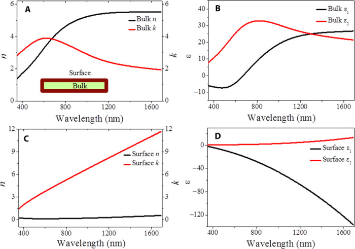
(A) Refractive index, n, and extinction coefficient, k, of the insulating bulk of topological insulator BSTS crystals. The inset shows the intrinsic structures of topological insulator BSTS single crystals with surface states and bulk states. (B) Dielectric function, ε, of the insulating bulk of topological insulator BSTS nanocones. (C) Refractive index, n, and extinction coefficient, k, of the metallic surface of topological insulator BSTS crystals. (D) Dielectric function, ε, of the metallic surface of topological insulator BSTS crystals.
Nanofabrication of nanocone arrays
Periodic nanocone arrays were directly patterned on the top surface of cleaved BSTS crystal sheets using a focused ion-beam system. Because the nanofabrication process does not break the lattice structures, the nanocones can be considered as BSTS nanocrystals with topological surface states. The lateral dimension of each fabricated sample was 100 × 100 μm. The base diameter (d) of nanocones ranges from 200 to 600 nm. The height (h) of the BSTS nanocones is fixed at 450 nm. The period (p) of the nanocone array ranges from 400 to 1300 nm. Figure 2A displays a schematic drawing of an intrinsically core-shell nanostructure of a bulk-insulating topological insulator BSTS nanocone. The red part is the metallic shell with a thickness of ~1.5 nm (22). The yellow part is the dielectric core with a band gap of 0.25 eV (22). Such a band gap is much higher than the thermal energy at room temperature (~0.025 eV), which guarantees the insulating bulk states at room temperature. Figure 2B shows a 3D atomic force microscopy (AFM) image of the fabricated BSTS nanostructures, which displays a shape of nanocones. Figure 2C represents a 2D AFM image of the BSTS nanocone arrays with d = 300 nm and p = 600 nm. Figure 2D shows a 3D image of the BSTS nanocone arrays. The morphology of these arrays can also be clearly seen from the scanning electron microscopy (SEM) images (see fig. S2).
Fig. 2. Intrinsically core-shell topological insulator BSTS nanocone arrays fabricated on the surface of flat BSTS crystal sheets.
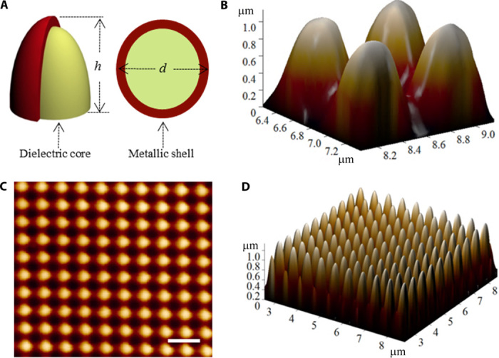
(A) A schematic drawing of intrinsically core-shell nanostructures of 3D topological insulator BSTS nanocones. The red part is a metallic shell, and the yellow part is a dielectric core. (B) An enlarged 3D AFM image of four BSTS nanocones with d = 300 nm and h = 450 nm. (C) A 2D AFM image of BSTS nanocone arrays with d = 300 nm, h = 450 nm, and p = 600 nm. The scale bar is 1000 nm. (D) A 3D AFM image of these BSTS nanocone arrays.
Plasmonic absorption measurements
The reflection spectra R(λ) of BSTS core-shell nanocone arrays were measured using a Fourier transform infrared (FTIR) microscope system. The measured wavelengths were from 300 to 800 nm, covering the visible frequency range. The absorption spectra were calculated by using the following formula: A(λ) = 1 − R(λ). Figure 3A shows the normalized absorption spectra A(λ) measured from the BSTS nanocone arrays with different values of d and p. No absorption peak was observed in the BSTS nanocone arrays with d = 200 nm. Evident plasmonic responses were observed from the arrays, with d ranging from 300 to 600 nm and p ranging from 600 to 1200 nm. The plasmonic absorption peaks shift from a wavelength of 300 to 600 nm with the increase of d, as shown in fig. S3. To further confirm the plasmonic responses, we fabricated BSTS nanocone arrays with fixed d = 500 nm and variant p ranging from 1000 to 1300 nm. As shown in Fig. 3B, the plasmonic absorption peaks shift from a wavelength of 420 to 460 nm. They are all located within the measured ε-negative regime of the permittivity in the BSTS bulk and surface.
Fig. 3. Plasmonic absorption spectra of core-shell BSTS nanocone arrays.
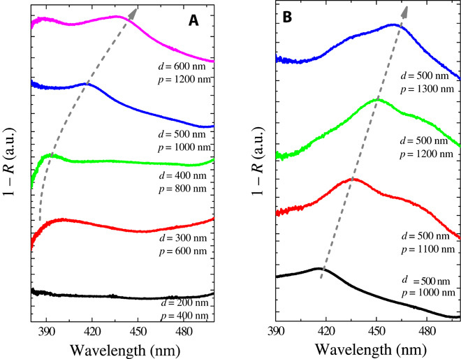
(A) Normalized absorption spectra (1 − R) of BSTS nanocone arrays with different p, ranging from 400 to 1200 nm. The nanocone base diameter (d) ranges from 200 to 600 nm. (B) Absorption spectra of BSTS nanocone arrays with fixed d = 500 nm and different p. The p parameter ranges from 1000 to 1300 nm.
The previously reported experimental observations of plasmonic absorptions in BSTS nanoslits and grating are polarization-sensitive (22). The plasmonic resonances can only propagate along the direction perpendicular to the nanoslits and grating. This limits their applications in some fields such as plasmonic solar cells and photodetectors. The plasmonic resonances in our fabricated intrinsically core-shell nanocone arrays are polarization-insensitive. They can be directly integrated into thin film photovoltaic devices for localizing and harvesting light.
Origin of plasmonic response
As mentioned earlier, Dirac plasmon excitations were initially observed in topological insulator Bi2Se3 micro-ribbon arrays in the infrared (terahertz) frequency range (21). Through theoretical calculations, the observed plasmons were assigned to Dirac quasi-particles at the topological surface. In addition, low-frequency conductance and mid-infrared absorption were investigated in the topological insulator (Bi1−x_In_x)2Se3 by using time-domain terahertz spectroscopy (31). The data showed room-temperature optical absorption at 0.31 eV, which implied a Dirac plasma frequency located in the mid-infrared frequency range. With a similar electron density, the plasmonic resonances of Dirac surface states in the topological insulator BSTS should also locate in the mid-infrared to terahertz frequency range. Therefore, the massless Dirac electrons in the surface states contribute very little to the visible plasmonic absorptions.
The optical conductivity contribution of bulk carriers of bismuth-based topological insulators was measured and investigated by optical spectroscopy (32, 33). The conductivity contribution from bulk carriers was found to be higher than that from the surface Dirac carriers. Therefore, the observed plasmonic absorptions in the visible region largely originate from interband absorption in the BSTS bulk states (22). The interband transition–induced negative permittivity was theoretically predicted in Bi2Se3 (34). BSTS may be the first topological insulator material in which the negative permittivity originates from the interband electronic absorption.
The previously reported plasmonic absorption in BSTS nanoslits and gratings cannot be well fitted without considering the contribution from surface states (22). In these nanostructures, the plasmonic response was attributed to the combined contributions of bulk charge carriers from interband transitions and surface charge carriers of the topological insulator BSTS. Analogously, in the core-shell nanocone arrays, massive electrons from the bulk on the nanoshell surface might also contribute in part to the observed plasmonic absorption in the visible frequency range. However, it should be noted that the present massive electrons on the nanoshell surface in the bulk states and the massless Dirac electrons in the surface states cannot be easily separated by model fitting.
Finite-difference time-domain simulations
The plasmonic absorption of the nanocone arrays was simulated by using the finite-difference time-domain (FDTD) software. The dielectric functions of the BSTS cores and shells used in the simulation are from the data shown in Fig. 1. A broadband plane wave source (300 to 800 nm) was used to simulate the light incident on the nanocone arrays from the top surface. Periodic boundary conditions were used at the lateral boundaries of the simulation model to mimic the infinite periodic arrays of nanoparticles. To quantify the absorption of the nanocone arrays, we first calculated the light reflection R(λ) from the nanocone arrays, and then the absorption can be achieved by A(λ) = 1 − R(λ). The reflection data were obtained from a power monitor set above the nanocone arrays with a height of 1 μm.
Figure 4 (A to D) shows the localized electromagnetic field distribution in BSTS nanocone arrays with different values of d and p. The d and p changes of nanocone arrays range from 300 to 600 nm and from 600 to 1200 nm, respectively. From the images of electromagnetic field distributions, we noticed that the plasmon resonances were localized on the surface of BSTS nanocones. From the FDTD simulation, we also found that the bulk states of BSTS largely contribute to the observed plasmonic responses. The electromagnetic field distributions in BSTS nanocone arrays with fixed d = 500 nm and different p are listed in fig. S4 (A to C). In addition, numerical simulation was also performed to calculate the plasmonic absorption spectra, which can be found in fig. S3. The simulated plasmonic absorption spectra fit well with the experimental results. The small discrepancy may result from the surface roughness of the fabricated core-shell nanocone arrays.
Fig. 4. FDTD simulation of the electromagnetic field distribution in BSTS nanocone arrays.
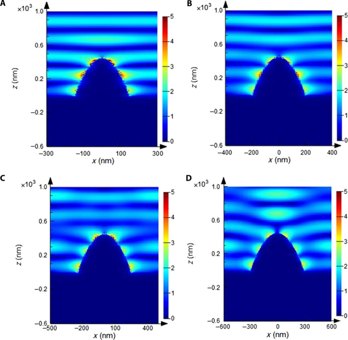
(A) Nanocone arrays with d = 300 nm and p = 600 nm at a wavelength of 395 nm. (B) Nanocone arrays with d = 400 nm and p = 800 nm at a wavelength of 406 nm. (C) Nanocone arrays with d = 500 nm and p = 1000 nm at a wavelength of 411 nm. (D) Nanocone arrays with d = 600 nm and p = 1200 nm at a wavelength of 430 nm. The plasmon resonances are localized and enhanced on the surfaces of BSTS nanocones.
Backward light scattering
With an ultrahigh bulk refractive index, the topological insulator BSTS has potential in effectively enhancing light absorption and controlling light scattering processes. We experimentally measured light scattering by the core-shell BSTS nanocone arrays using a home-built dark-field microscope. A white light was used as the source for the illumination. Figure 5A shows a schematic drawing of the home-built dark-field microscope used in the measurements. The images were captured using a confocal microscope. In the propagation process, the central light beam is blocked by the dark-field patch stop. Only a ring-shaped beam on the edge reaches the BSTS nanocone arrays, which is simultaneously reflected and scattered by the BSTS nanocone arrays.
Fig. 5. Backward light scattering by core-shell BSTS nanocone arrays.
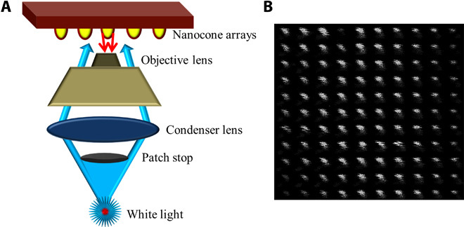
(A) A schematic diagram of a home-built dark-field microscope for light scattering measurements. The bottom of the system is the light source, and the black disc is a patch stop that blocks the central beam. The blue arrows represent incident light, and the red arrows represent the scattered light. Only scattered light can be detected by the objective lens. (B) Images of backward light scattering by the nanocone arrays with d = 300 nm and p = 600 nm. The bright spots are the strong scattered light.
The backward scattered light by the BSTS nanocone arrays was detected by the objective lens, whereas the reflected light was not detectable. Hence, the dark-field microscope was able to merely detect the scattered light and exclude the unscattered light from the nanocone arrays. Using such a microscope, we measured the backward light scattering of BSTS nanocone arrays with d = 300 nm and p = 600 nm. As shown in Fig. 5B, the captured black-and-white photo displays ordered bright spots, which suggest strong backward light scattering by the BSTS nanocone arrays. The scattering may originate from the integral effects of plasmonic scattering by metallic shells and Mie scattering by the high-index dielectric cores.
Applications in plasmonic solar cells
BSTS nanocone arrays combine the excellent properties of plasmonic metallic nanostructures and high–refractive index dielectric nanostructures. They demonstrate both localized surface plasmonic resonances and strong light scattering. Hence, the performance of light manipulation can be markedly improved in the subwavelength and broad wavelength ranges. In addition, unlike the plasmonic metallic nanostructures, BSTS nanocone arrays do not cause large parasitic loss and electrical property deterioration. Hence, the intrinsically core-shell nanostructure is highly promising for low-loss and high-performance optical devices.
Because the plasmonic resonances in the nanocone arrays locate in the visible frequency, integrating them into photovoltaic devices is expected to achieve enhanced light absorption and efficiency (7). The strong backward scattering in BSTS nanocone arrays also enables the enhancement of optical absorption when they are placed at the back of photovoltaic devices (9). Because of the large backward scattering angles, this could achieve a much larger light path length, which is extremely beneficial for photovoltaic devices. Using the FDTD method, we theoretically simulated the absorption enhancement of light in a 300-nm-thick a-Si solar cell. The configuration of the proposed a-Si thin film solar cells is shown in Fig. 6A. With the integration of topological insulator nanoparticles, a large light absorption enhancement was achieved at both the short wavelength and long wavelength regions. This led to a 15% enhancement of light absorption in the whole wavelength region and up to 55% enhancement at a wavelength of 325 nm. These results indicate the potential application of the topological insulator nanocone arrays in solar cell technology.
Fig. 6. Plasmon resonances enhanced light absorption in ultrathin a-Si solar cells simulated using FDTD.
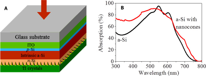
(A) Configuration of a-Si solar cells with core-shell BSTS nanocone arrays integrated into the back of a-Si thin films. The BSTS particles replace Al as the back electrodes of solar cells. (B) Optical absorptions in a-Si thin-film solar cells without (black curve) and with (red curve) BSTS nanocone arrays. The BSTS nanocone arrays achieve broadband enhancements of light absorptions in the visible frequency range.
DISCUSSION
The topological insulator BSTS nanocone is a novel type of plasmonic nanostructure that has an intrinsically core-shell formation and demonstrates visible-range plasmonic responses, strong backward light scattering, and an ultrahigh bulk refractive index. Compared to traditional core-shell nanostructures that are all artificial, the core-shell structure of BSTS nanocones is intrinsic (35). In addition, with plasmonic responses in the mid-infrared to terahertz range in the topological surface states and in the blue ultraviolet to visible range in the bulk states, topological insulator nanostructures provide an excellent platform for realizing ultra-broadband plasmon excitations in one material. Hence, topological insulator nanostructures could be extensively used in a variety of optical devices, such as ultra-broadband photodetectors.
Refractive index is one of most important optical constants in almost all optical devices, such as lenses, waveguides, and optical fibers (36). The refractive index in the core of BSTS nanostructures is much higher than that of well-known conventional high-index materials, such as Si (~3.5) and Ge (~4), at near-infrared frequencies. With an ultrahigh refractive index, BSTS nanocones are promising for realizing controllable electric and magnetic resonances as well as directional light scattering. In addition, topological insulator materials also demonstrate a high, near-infrared transparency of more than 70% over a wide range of wavelengths (37). On the basis of these features, topological insulator nanostructures may have practical applications in high-efficiency optical devices, such as visible-region nanoantennas and antireflection coating (38, 39).
CONCLUSION
In summary, we have proposed and fabricated a new type of core-shell plasmonic nanostructures with an ultrahigh bulk refractive index based on topological insulator materials. The plasmonic responses of the new nanostructures locate in the visible frequency range and can be tuned by changing the size and period of the nanocone arrays. Strong backward light scattering caused by plasmonic resonances and dielectric cores was also observed in the visible frequency range. Both the plasmonic resonances and the strong backward light scattering in the BSTS nanocone arrays are extremely beneficial for low-loss and high-performance optical devices, such as solar cells. Hence, our work paves the way for practical applications of topological insulator nanostructures in advanced optical and plasmonic devices.
MATERIALS AND METHODS
Single crystal growth
The bulk BSTS single crystals were grown using a modified Bridgeman method (26). High-purity (99.9999%) Bi, Sb, Te, and Se were mixed at a molar ratio of 1.5:0.5:1.8:1.2 in an evacuated quartz tube. The quartz tube was placed in a box special furnace with a temperature gradient of 5° to 10°/cm. The furnace temperature was increased and maintained at 950°C for 1 week and then gradually decreased to room temperature over 3 weeks. The grown crystals had smooth and shiny surfaces and were easily cleaved.
Nanofabrication
Nanocone arrays were directly patterned on the top surface of cleaved BSTS crystal sheets using a focused ion-beam system (Raith IonLiNE). The nanostructures of nanocone arrays were realized by fabricating two crossed grating with variant periods. The ion density was fixed to keep the height of nanocones constant. The lateral dimension of each fabricated sample was 100 × 100 μm.
Optical measurements
The refractive index and extinction efficiency of flat BSTS single crystals were measured using a spectroscopic ellipsometer (J. A. Woollam Co.). The optical constants were fitted using the models in the software. The reflection spectra were measured using an FTIR microscope (Bruker LUMOS). The measured wavelengths were from 300 to 800 nm. The light scattering was measured using a home-built dark-field microscope. A white light was used as the light source. A ring-shaped patch was used to block the central beam.
FDTD simulations
The plasmonic absorption was simulated using FDTD software (Lumerical Solutions). FDTD was also used to theoretically simulate the absorption enhancement of light in ultrathin a-Si solar cells.
Supplementary Material
http://advances.sciencemag.org/cgi/content/full/2/3/e1501536/DC1
Acknowledgments
We thank H. Ren, X. Li, X. Yang, and Q. Zhang for technical assistance, and H. Lu and X. Wang for helpful discussions. Funding: M.G. acknowledges the support from the Australian Research Council (ARC) through the Discovery Project (DP140100849) and the Centre of Excellence for Ultrahigh-bandwidth Devices for Optical Systems (CUDOS) (CE110001018). X.W. acknowledges the partial support from the ARC through the Discovery Project (DP130102956) and the ARC Future Fellowship project (FT130100778). Author contributions: Z.Y. and M.G. conceived the idea and wrote the manuscript. Z.Y. fabricated the nanostructures and conducted the experimental measurements and data analysis. B.C. conducted the theoretical simulation. L.W. and X.W. guided the synthesis of bulk crystals. All authors contributed to the writing of the manuscript and the discussion of the results. Competing interests: The authors declare that they have no competing interests. Data availability: All data needed to evaluate the conclusions in the paper are present in the paper and/or the Supplementary Materials. Additional data related to this paper may be requested from the authors.
SUPPLEMENTARY MATERIALS
Supplementary material for this article is available at http://advances.sciencemag.org/cgi/content/full/2/3/e1501536/DC1
Fig. S1. XRD of BSTS bulk crystals with growing orientation along (001).
Fig. S2. SEM images of topological insulator BSTS nanocone arrays.
Fig. S3. FDTD simulation of plasmonic absorption spectra in BSTS nanocone arrays.
Fig. S4. FDTD simulation of electromagnetic field distribution in BSTS nanocone arrays.
Fig. S5. Wavelengths of the absorption resonance peaks as a function of the base diameter d of BSTS nanocones.
REFERENCES AND NOTES
- 1.S. A. Maier, Plasmonics: Fundamentals and Applications (Springer Science & Business Media, US, 2007). [Google Scholar]
- 2.Fang Z., Zhu X., Plasmonics in nanostructures. Adv. Mater. 25, 3840–3856 (2013). [DOI] [PubMed] [Google Scholar]
- 3.Zijlstra P., Chon J. W. M., Gu M., Five-dimensional optical recording mediated by surface plasmons in gold nanorods. Nature 459, 410–413 (2009). [DOI] [PubMed] [Google Scholar]
- 4.Li X., Lan T.-H., Tien C.-H., Gu M., Three-dimensional orientation-unlimited polarization encryption by a single optically configured vectorial beam. Nat. Commun. 3, 998 (2012). [DOI] [PMC free article] [PubMed] [Google Scholar]
- 5.Maier S. A., Kik P. G., Atwater H. A., Meltzer S., Harel E., Koel B. E., Requicha A. A.G., Local detection of electromagnetic energy transport below the diffraction limit in metal nanoparticle plasmon waveguides. Nat. Mater. 2, 229–232 (2003). [DOI] [PubMed] [Google Scholar]
- 6.Anker J. N., Hall W. P., Lyandres O., Shah N. C., Zhao J., Van Duyne R. P., Biosensing with plasmonic nanosensors. Nat. Mater. 7, 442–453 (2008). [DOI] [PubMed] [Google Scholar]
- 7.Atwater H. A., Polman A., Plasmonics for improved photovoltaic devices. Nat. Mater. 9, 205–213 (2010). [DOI] [PubMed] [Google Scholar]
- 8.Chen X., Jia B., Saha J. K., Cai B., Stokes N., Qiao Q., Wang Y., Shi Z., Gu M., Broadband enhancement in thin-film amorphous silicon solar cells enabled by nucleated silver nanoparticles. Nano Lett. 12, 2187–2192 (2012). [DOI] [PubMed] [Google Scholar]
- 9.Zhang Y., Stokes N., Jia B., Fan S., Gu M., Toward ultra-thin plasmonic silicon wafer solar cells with minimized efficiency loss. Sci. Rep. 4, 4939 (2014). [DOI] [PMC free article] [PubMed] [Google Scholar]
- 10.Kang G., Yoo J., Ahn J., Kim K., Transparent dielectric nanostructures for efficient light management in optoelectronic applications. Nano Today 10, 22–47 (2015). [Google Scholar]
- 11.Brongersma M. L., Cui Y., Fan S., Light management for photovoltaics using high-index nanostructures. Nat. Mater. 13, 451–460 (2014). [DOI] [PubMed] [Google Scholar]
- 12.Zhao Q., Zhou J., Zhang F., Lippens D., Mie resonance-based dielectric metamaterials. Mater. Today 12, 60–69 (2009). [Google Scholar]
- 13.Fink Y., Winn J. N., Fan S., Chen C., Michel J., Joannopoulos J. D., Thomas E. L., A dielectric omnidirectional reflector. Science 282, 1679–1682 (1998). [DOI] [PubMed] [Google Scholar]
- 14.Cao L., White J. S., Park J.-S., Schuller J. A., Clemens B. M., Brongersma M. L., Engineering light absorption in semiconductor nanowire devices. Nat. Mater. 8, 643–647 (2009). [DOI] [PubMed] [Google Scholar]
- 15.Lin D., Fan P., Hasman E., Brongersma M. L., Dielectric gradient metasurface optical elements. Science 345, 298–302 (2014). [DOI] [PubMed] [Google Scholar]
- 16.Yan J. H., Liu P., Lin Z. Y., Wang H., Chen H. J., Wang C. X., Yang G. W., Magnetically induced forward scattering at visible wavelengths in silicon nanosphere oligomers. Nat. Commun. 6, 7042 (2015). [DOI] [PMC free article] [PubMed] [Google Scholar]
- 17.Fu Y. H., Kuznetsov A. I., Miroshnichenko A. E., Yu Y. F., Luk’yanchuk B., Directional visible light scattering by silicon nanoparticles. Nat. Commun. 4, 1527 (2013). [DOI] [PubMed] [Google Scholar]
- 18.Valentine J., Li J., Zentgraf T., Bartal G., Zhang X., An optical cloak made of dielectrics. Nat. Mater. 8, 568–571 (2009). [DOI] [PubMed] [Google Scholar]
- 19.Hasan M. Z., Kane C. L., Colloquium: Topological insulators. Rev. Mod. Phys. 82, 3045–3067 (2010). [Google Scholar]
- 20.Qi X.-L., Zhang S.-C., Topological insulators and superconductors. Rev. Mod. Phys. 83, 1057–1110 (2011). [Google Scholar]
- 21.Di Pietro P., Ortolani M., Limaj O., Di Gaspare A., Giliberti V., Giorgianni F., Brahlek M., Bansal N., Koirala N., Oh S., Calvani P., Lupi S., Observation of Dirac plasmons in a topological insulator. Nat. Nanotechnol. 8, 556–560 (2013). [DOI] [PubMed] [Google Scholar]
- 22.Ou J.-Y., So J.-K., Adamo G., Sulaev A., Wang L., Zheludev N. I., Ultraviolet and visible range plasmonics in the topological insulator Bi1.5Sb0.5Te1.8Se1.2. Nat. Commun. 5, 5139 (2014). [DOI] [PubMed] [Google Scholar]
- 23.Ando Y., Topological insulator materials. J. Phys. Soc. Jpn. 82, 102001 (2013). [Google Scholar]
- 24.Jozwiak C., Park C.-H., Gotlieb K., Hwang C., Lee D.-H., Louie S. G., Denlinger J. D., Rotundu C. R., Birgeneau R. J., Hussain Z., Lanzara A., Photoelectron spin-flipping and texture manipulation in a topological insulator. Nat. Phys. 9, 293–298 (2013). [Google Scholar]
- 25.Kong D., Chen Y., Cha J. J., Zhang Q., Analytis J. G., Lai K., Liu Z., Hong S. S., Koski K. J., Mo S.-K., Hussain Z., Fisher I. R., Shen Z.-X., Cui Y., Ambipolar field effect in the ternary topological insulator (BixSb1−x)2Te3 by composition tuning. Nat. Nanotechnol. 6, 705–709 (2011). [DOI] [PubMed] [Google Scholar]
- 26.Xia B., Ren P., Sulaev A., Liu P., Shen S.-Q., Wang L., Indications of surface-dominated transport in single crystalline nanoflake devices of topological insulator Bi1.5Sb0.5Te1.8Se1.2. Phys. Rev. B 87, 085442 (2013). [Google Scholar]
- 27.Tang C. S., Xia B., Zou X., Chen S., Ou H.-W., Wang L., Rusydi A., Zhu J.-X., Chia E. E. M., Terahertz conductivity of topological surface states in Bi1.5Sb0.5Te1.8Se1.2. Sci. Rep. 3, 3513 (2013). [DOI] [PMC free article] [PubMed] [Google Scholar]
- 28.Arakane T., Sato T., Souma S., Kosaka K., Nakayama K., Komatsu M., Takahashi T., Ren Z., Segawa K., Ando Y., Tunable Dirac cone in the topological insulator Bi2−xSbxTe3−ySey. Nat. Commun. 3, 636 (2012). [DOI] [PubMed] [Google Scholar]
- 29.Johs B., Hale J. S., Dielectric function representation by B-splines. Phys. Status Solidi A 205, 715–719 (2008). [Google Scholar]
- 30.Jellison G. E. Jr, Modine F. A., Parameterization of the optical functions of amorphous materials in the interband region. Appl. Phys. Lett. 69, 371–373 (1996). [Google Scholar]
- 31.Wu L., Brahlek M., Valdés Aguilar R., Stier A. V., Morris C. M., Lubashevsky Y., Bilbro L. S., Bansal N., Oh S., Armitage N. P., A sudden collapse in the transport lifetime across the topological phase transition in (Bi1−xInx)2Se3. Nat. Phys. 9, 410–414 (2013). [Google Scholar]
- 32.Akrap A., Tran M., Ubaldini A., Teyssier J., Giannini E., van der Marel D., Lerch P., Homes C. C., Optical properties of Bi2Te2Se at ambient and high pressures. Phys. Rev. B 86, 235207 (2012). [Google Scholar]
- 33.Di Pietro P., Vitucci F. M., Nicoletti D., Baldassarre L., Calvani P., Cava R., Hor Y. S., Schade U., Lupi S., Optical conductivity of bismuth-based topological insulators. Phys. Rev. B 86, 045439 (2012). [Google Scholar]
- 34.Sharma Y., Srivastava P., Dashora A., Vadkhiya L., Bhayani M. K., Jain R., Jani A. R., Ahuja B. L., Electronic structure, optical properties and Compton profiles of Bi2S3 and Bi2Se3. Solid State Sci. 14, 241–249 (2012). [Google Scholar]
- 35.Gawande M. B., Goswami A., Asefa T., Guo H., Biradar A. V., Peng D.-L., Zborila R., Varmaf R. S., Core–shell nanoparticles: Synthesis and applications in catalysis and electrocatalysis. Chem. Soc. Rev. 44, 7540–7590 (2015). [DOI] [PubMed] [Google Scholar]
- 36.Singh S., Refractive index measurement and its applications. Phys. Scripta 65, 167 (2001). [Google Scholar]
- 37.Peng H., Dang W., Cao J., Chen Y., Wu D., Zheng W., Li H., Shen Z.-X., Liu Z., Topological insulator nanostructures for near-infrared transparent flexible electrodes. Nat. Chem. 4, 281–286 (2012). [DOI] [PubMed] [Google Scholar]
- 38.Zhang S., Jiang R., Xie Y.-M., Ruan Q., Yang B., Wang J., Lin H.-Q., Colloidal moderate-refractive-index Cu2O nanospheres as visible-region nanoantennas with electromagnetic resonance and directional light-scattering properties. Adv. Mater. 27, 7432–7439 (2015). [DOI] [PubMed] [Google Scholar]
- 39.Spinelli P., Verschuuren M. A., Polman A., Broadband omnidirectional antireflection coating based on subwavelength surface Mie resonators. Nat. Commun. 3, 692 (2012). [DOI] [PMC free article] [PubMed] [Google Scholar]
Associated Data
This section collects any data citations, data availability statements, or supplementary materials included in this article.
Supplementary Materials
http://advances.sciencemag.org/cgi/content/full/2/3/e1501536/DC1
Supplementary material for this article is available at http://advances.sciencemag.org/cgi/content/full/2/3/e1501536/DC1
Fig. S1. XRD of BSTS bulk crystals with growing orientation along (001).
Fig. S2. SEM images of topological insulator BSTS nanocone arrays.
Fig. S3. FDTD simulation of plasmonic absorption spectra in BSTS nanocone arrays.
Fig. S4. FDTD simulation of electromagnetic field distribution in BSTS nanocone arrays.
Fig. S5. Wavelengths of the absorption resonance peaks as a function of the base diameter d of BSTS nanocones.