Reverse-engineering the Yamaha DX7 synthesizer's sound chip from die photos (original) (raw)
The Yamaha DX7 digital synthesizer was released in 1983 and became "one of the most important advances in the history of modern popular music"1. It defined the sound of 1980s pop music, used by bands from A-ha and Michael Jackson to Dolly Parton and Whitney Houston. The DX7's electric piano sound can be heard in over 40% of 1986's top hits.2Compared to earlier synthesizers, the DX7 was compact, inexpensive, easy to use, and provided a new soundscape.3
While digital synthesis is straightforward nowadays, microprocessors4weren't fast enough to do this in the early 1980s. Instead, the DX7 used two custom chips: the YM21290 EGS "envelope" chip generated frequency and envelope data, which it fed to the YM212805 OPS "operator" chip that generated the sound waveforms. In this blog post, I investigate the operator chip and how it digitally produced sounds using a technique called FM synthesis.6 21
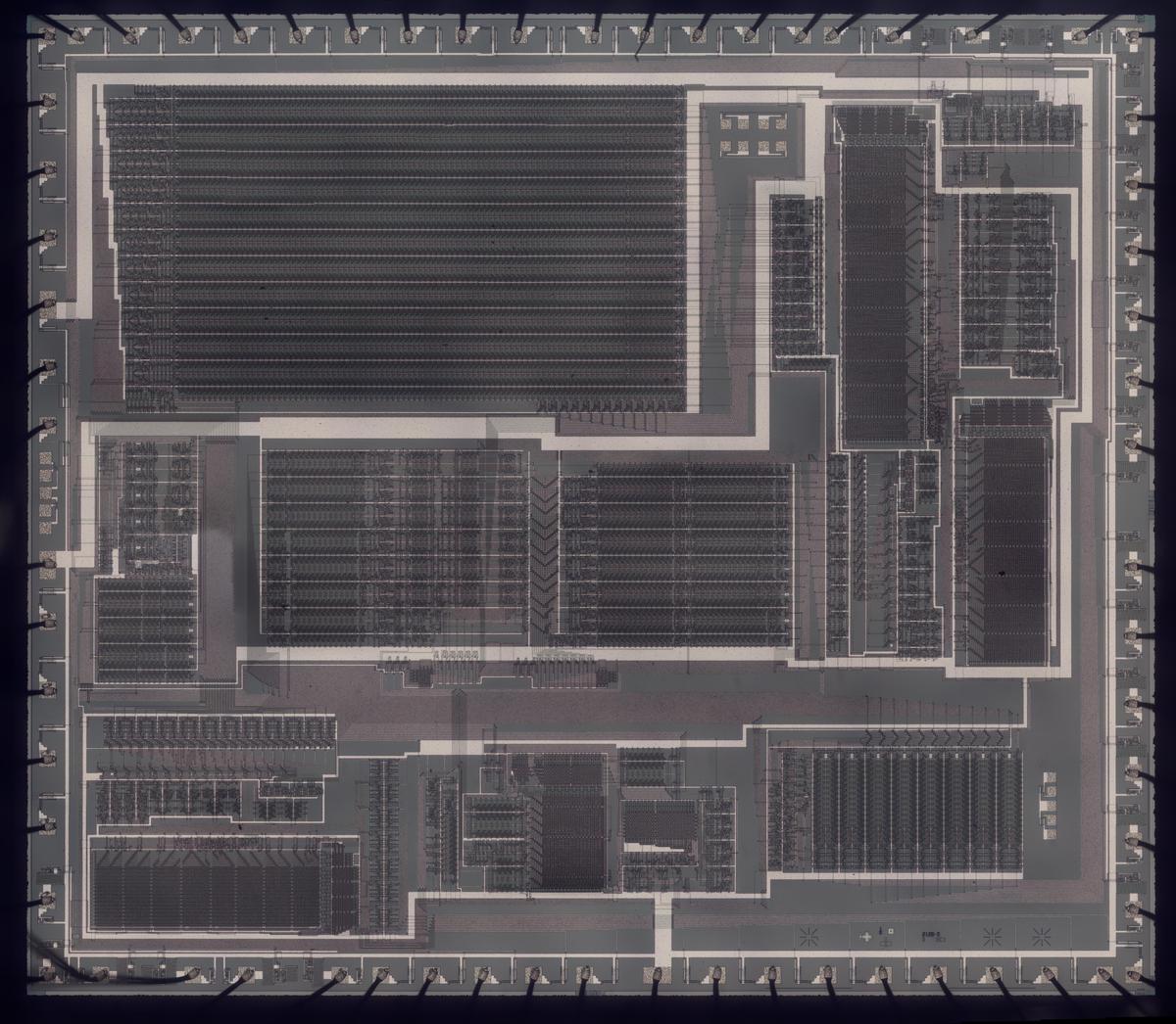
I created the high-resolution die photo below by compositing over a hundred microscope photos.6Around the edges, you can see the 64 bond wires attached to pads; these connect the silicon die to the chip's 64 pins. The chip has one layer of metal, visible as the whitish lines on top. (Power and ground are the thick metal lines.) Underneath the metal, the polysilicon wiring layer appears reddish or greenish. Finally, the underlying silicon is grayish. The overall layout of the chip is dense rectangles of circuitry with the space between them used for signal routing. I will discuss these circuitry blocks in detail below.
Die photo of the DX7's YM21280 Operator chip. Click this photo (or any other) for a magnified version.
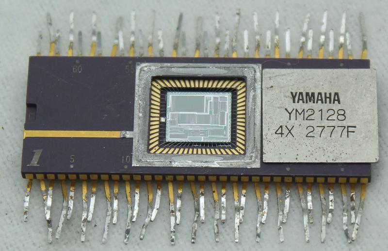
The photo below shows the integrated circuit with the metal lid removed, showing the silicon die inside. The pins have been flattened in the photo; they are normally bent downwards, but in a staggered pattern.7 The four rows of pins make this a quad in-line package, with twice the pin density as a regular DIP chip. As a result, this 64-pin chip has a smaller package than a standard 40-pin DIP chip.
The integrated circuit package with the metal lid removed, revealing the silicon die. Pin numbers are printed on the package, which is unusual.
Analog and digital
In the 1960s and 1970s, synthesizers were mostly analog.8An oscillator was controlled by the keyboard, generating a wave at the appropriate frequency. This signal was fed through a filter, which shaped the frequency spectrum to produce the desired tone quality (timbre). Finally, the signal had its volume shaped by an envelope generator that made the volume ramp up when the key was pressed, and die off gradually when the key was released.9
An analog synthesizer was built from components such as resistors, capacitors, and op-amps, with analog voltages as the signals. One problem was that the analog synthesizers needed to be tuned since these component values could drift over time. Another problem was that the complex circuitry generated one note, so analog synthesizers were typically monophonic, producing a single note at a time. The functions of an analog synthesizer were typically controlled by patch cords, potentiometer knobs, and switches, which allowed a wide variety of sounds to be produced. This made it difficult to select the desired sound, since all the parameters needed to be set manually.
Digital synthesis provided a completely different way of generating sounds. The sound values were produced digitally by an algorithm that generated numeric values. These values were converted to the output signal voltages by a digital-to-analog converter (DAC). Digital synthesizers solved many of the problems of analog synthesis: they could easily play multiple notes at once (i.e. polyphony), configurations could be stored as digital files, they could be controlled digitally10, they replaced precision analog components with cheaper digital circuits, and they produced new classes of sounds. The DX7 wasn't the first digital synthesizer, but it was the first to achieve commercial success. It became one of the best-selling synthesizers ever, with over 150,000 sold.
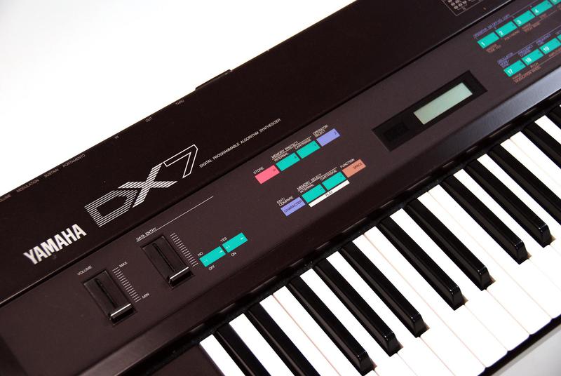
The Yamaha DX7 synthesizer with its 61-key keyboard and digital controls. Photo by rockheim (CC BY-NC-SA 2.0).
FM synthesis
The DX7 uses FM synthesis to generate its sounds.11The idea is that you start with a sine wave (the carrier signal) and perturb it with another signal (the modulating signal). The modulating signal changes the phase (and thus the frequency) of the carrier, creating complex harmonic structures.
The digital implementation of frequency modulation starts with a lookup table that holds a digitized sine wave. By stepping an index through the table at a specific rate, you can produce a sine wave of a fixed frequency. To make this concrete, suppose the table is 4096 entries long and the index is updated at 40960 Hertz. If you increment the index by 100 each time, you'll cycle through the table 1000 times every second, so a sine wave at 1 kHz will be produced. The index represents the phase of the signal: as the index moves through the table, this corresponds to a phase of 0 to 2π and an output of sin(0) through sin(2π). Changing the increment value controls the frequency. For instance, an increment of 44 would produce 440 Hz.12
The next step is to modulate the output by adding a modulation signal to the index. When the modulation signal increases, the index will move through the table faster, increasing the output frequency. When the modulation signal decreases, the index will step through more slowly, decreasing the output frequency.
Digital synthesis can be implemented with straightforward hardware: a sine-wave table, an increment value that controls the frequency, and an adder that adds the increment to the table index (phase angle) each time step. Frequency modulation can be implemented by another adder to add the modulation value to the table index (phase angle).
The interactive tool below illustrates FM synthesis and the effects of changing the modulation frequency and amount of modulation.13The modulation signal is shown in yellow and the output is shown in red. (The carrier is fixed at 440 Hz.) Low levels of modulation distort the output waveform, while high levels create very complex waveforms. If the modulation and carrier frequencies have integer ratios, the output is periodic. But a detuned modulation frequency results in a complex, more bell-like sound.
Modulation level: 1
Modulation frequency ratio: 2
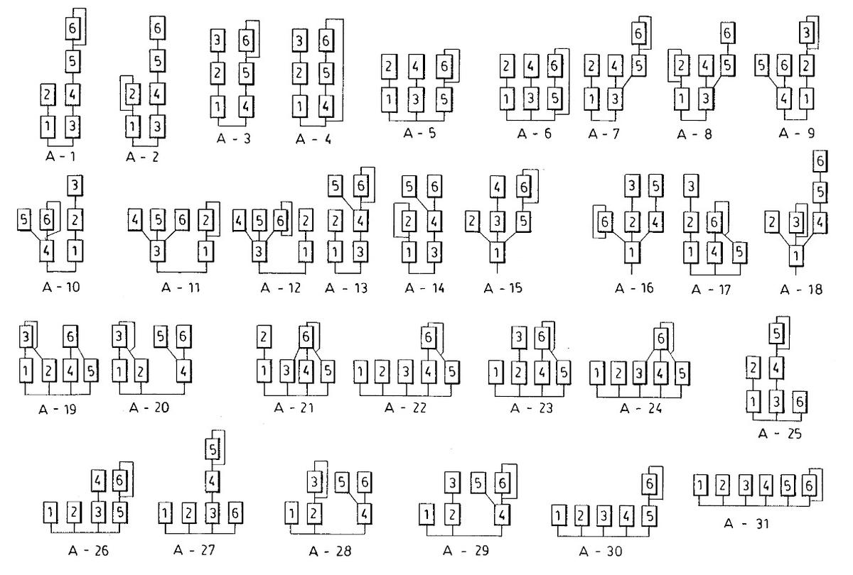
As you can see, a single modulator produces a variety of timbres and complex, unpredictable waveforms. However, the DX7 provides multiple modulators combined in various ways, making the sounds vastly more varied. For each note, the DX7 provides six oscillators (called operators) that can be combined in 32 different ways (called algorithms), shown below. For example, in algorithm 1, operator 6 modulates operator 5 which modulates operator 4 which modulates operator 3, which produces a sound. Meanwhile, operator 2 modulates operator 1, producing a second sound. Other algorithms combine the six operators in different ways. The level of each operator is controlled by a different envelope, so the note's timbre can evolve in complex ways over time.14
A chart of the DX7's algorithms, from the patent.
Inside the DX7
The DX7 can play 16 notes at once and each note has 6 operators, so there are 96 oscillators/operators in total. However, the circuitry operates sequentially, updating one oscillator and computing one operator at a time. The DX7 stores the current index (phase) values for each of the 96 oscillators but shares the circuitry that uses these values. Instead of RAM, the DX7 uses shift registers to hold data, in particular 96-stage shift registers to hold the 96 phase values. This approach drastically reduces the hardware requirements compared to using 96 separate oscillator circuits.
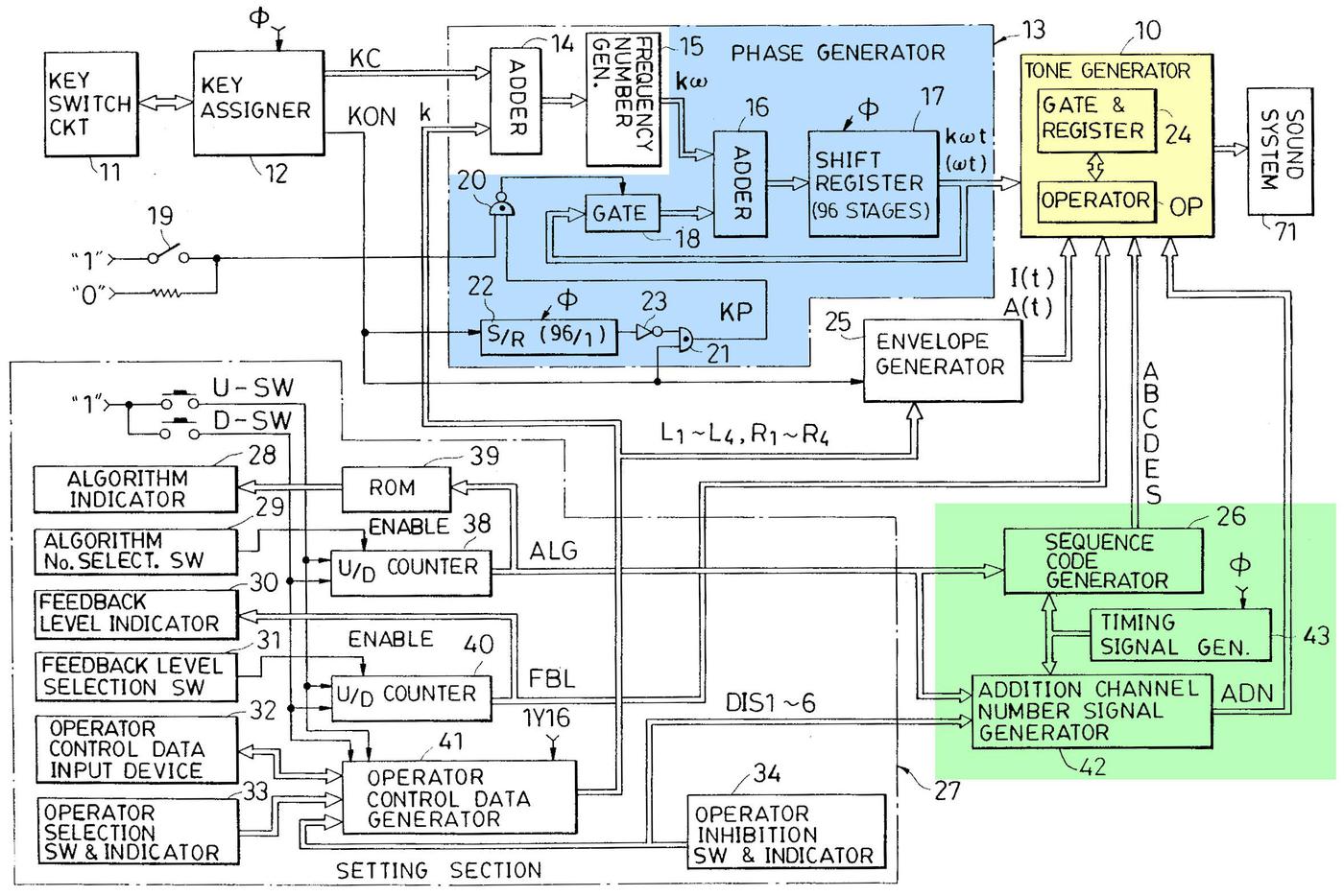
The diagram below shows the main architectural components of the DX7, with the components implemented in the operator chip highlighted. (The diagram, from the patent, is complicated but it shows the important features.) In the upper left, the keyboard circuitry detects when a key is played, generating a key code (KC), and a key-on signal (KON). The key code determines the frequency number, the increment used to compute the phase. The phase generator (blue) adds the increment to compute the phase, and the tone generator (yellow) produces the output sound value. The setting section in the lower left provides the user interface to configure the synthesizer. In the lower right (green), the sequence control generator sends control signals to the tone generator to implement the selected algorithm.
Architecture diagram of the DX7, from the patent.
In more detail, the phase generator (blue) implements the phase counters for the 96 digital oscillators. The "frequency number generator" in the envelope chip provides the increment values to the adder. The phase values are stored in the 96-stage shift register. The tone generator (yellow) is where the modulation happens. It takes the phase values, modulates them, and converts them to sine waves, producing the output sound value. It also modifies the level of the signals, as specified by the envelope generator. The sequence code generator (green) generates control signals (A, B, C, D, E, S) that select how modulation takes place at each step. The implementation of these components will be described in more detail below.
Logarithms and exponentials
The chip uses logarithms and exponentials for many of the internal values. The underlying problem is that multiplication is much harder to perform with hardware than addition, especially with 1980s-era technology. The solution is that the chip uses base-2 logarithms in many places because adding logarithms is equivalent to multiplying the values. (The chip uses lookup ROMs in combination with bit shifting to obtain the logarithms and exponentials.)
The first role for logarithms is in the frequency input to the chip: instead of a phase increment value, it receives the base-2 logarithm of the increment. The motivation is that note frequencies are related exponentially: for instance, going up one octave doubles the frequency. Thus, shifting a note requires multiplying the frequency. Since the envelope chip represents frequencies as logarithms, the multiplication becomes a quick addition. The envelope chip then passes the corresponding phase increment to the operator chip as a logarithmic value. The operator chip uses an exponential look-up ROM to convert this value back to a linear value.
The second role for logarithms is to apply the envelope that shapes the signal's amplitude. The envelope is a time-varying multiplicative scale factor, scaling the amplitude to, say, 70% or 30%. To avoid multiplication, the logarithm of the scale factor and the logarithm of the signal are added. A second exponential look-up ROM converts the result back to a linear value. The envelope is provided to the operator chip by the envelope chip in logarithmic form. The logarithm of the sine-wave signal is conveniently obtained by storing log2(sin(x)) in the waveform ROM instead of sin(x), so the logarithm is obtained "for free".15
A look at the die
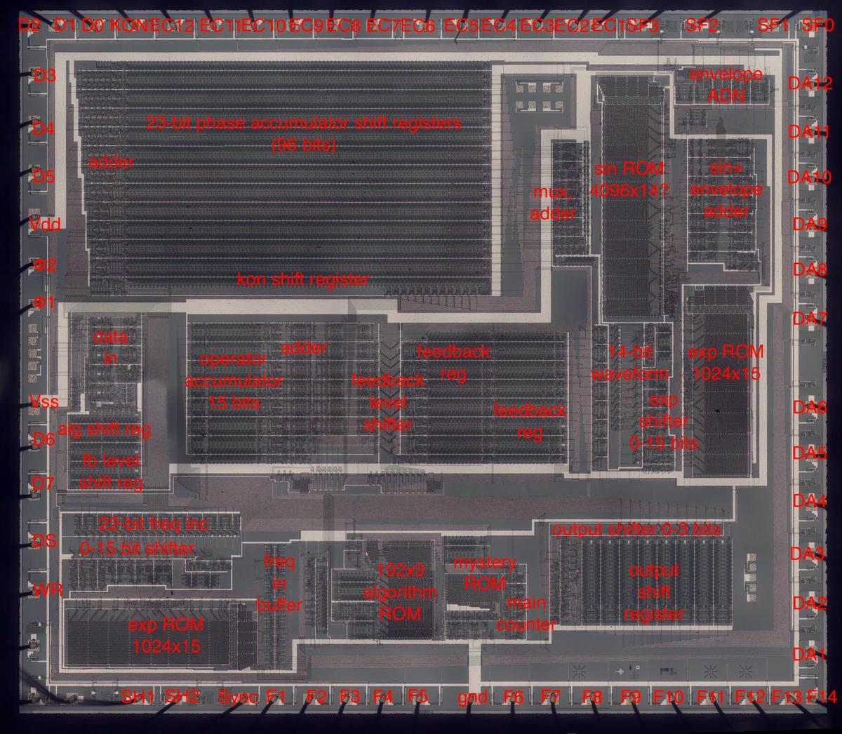
The diagram below labels the pins and the main functional blocks of the chip. The shift registers are the largest blocks of the chip, especially the phase shift registers in the upper left. ROMs are the second-largest blocks, especially the sine ROM and the two identical exponential ROMs. Adders provide most of the logic circuitry; there isn't much "random" logic compared to a processor chip, for instance. The chip has several bit shifters that shift a numeric value, multiplying or dividing it by a power of two.16In this section, I look at the low-level circuitry of the die and how the functions are implemented.
Die with the pins and major functional blocks labeled. (Click for a larger version.)
Shift registers
The main component of the chip is storage: the parameters for each operator, the phase counters for each oscillator, the output values for each note, and so forth. The storage is not implemented as RAM or fixed registers as you might expect, but as loops of shift registers with bits constantly moving in a cycle. The idea of a shift register is that it consists of a number of stages, say 16. During each clock cycle, the bits are shifted, with each bit moving to the next stage. One bit exits the shift register. This bit (or a new bit) can be fed into the shift register input, and it will appear at the output 16 clock cycles later.
Since the circuitry works on one oscillator/operator at a time in fixed order, shift registers are an efficient way of storing data and providing it at the right time, without the need for addressing logic. In other words, during each time interval, the appropriate data pops out of the shift registers for processing. The data (unmodified or modified as appropriate) is then fed back into the inputs of the shift register to pass through another cycle.
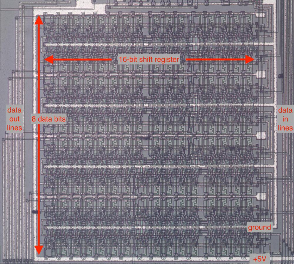
For example, each of the 16 notes requires 8 bits of configuration storage: 5 to specify the algorithm and 3 to specify the feedback level. This storage is implemented with 8 shift registers, each 16-bits long, as shown below. To select an algorithm, the external CPU writes the appropriate value into the shift register. Note that unlike RAM, entries in the shift register cannot be read and written arbitrarily. The system can only use values when they appear on the shift register output.
The configuration data shift registers are organized as eight 16-bit shift registers.
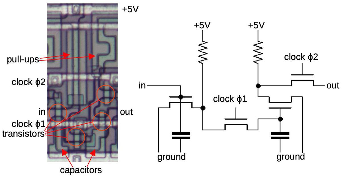
The schematic below shows how one stage of the shift register is implemented. The chip uses a two-phase clock. In the first phase, clock ϕ1 goes high, turning on the first transistor. The input signal goes through the inverter, through the transistor, and the voltage is stored in the capacitor. In the second phase, clock ϕ2 goes high, turning on the second transistor. The value stored in the capacitor goes through the second inverter, through the second transistor, and to the output, where it enters the next shift register stage. Thus, in one clock cycle (ϕ1 and then ϕ2), the input bit is transferred to the output. (The circuit is similar to dynamic RAM in the sense that bits are stored in capacitors. The clock needs to cycle before the charge on the capacitor drains away and data is lost. The inverters amplify and regenerate the bit at each stage.)
Schematic of one stage of the shift register.
The diagram below shows the physical implementation of one shift register stage. It's a bit confusing because there are three layers: the whitish metal on top, doped silicon regions on the bottom (which appear outlined in black), and polysilicon lines in the middle (which appear reddish or greenish). Transistors are formed when a polysilicon line crosses doped silicon. A capacitor is created similarly, with a polysilicon line and doped silicon forming the two plates of the capacitor. An inverter is created from a transistor that pulls the output to ground, along with a pull-up resistor. (The pull-up resistor is actually another transistor, specially doped to make it a depletion transistor.)
Implementation of one bit of the shift register. This matches the earlier schematic, but shows the components of the inverters.
ROMs
The next building block of the chip is ROM storage, used for the numeric look-up tables and other purposes. One ROM computes the log2 sine for the waveform. The chip has two identical exponential ROMs computing 2x. One converts the log-frequency increment value into a linear increment value. The second converts the log waveform value into a linear waveform value. An algorithm ROM defines the 32 algorithms, specifying the behavior of each of the 6 operators in each algorithm. Another ROM changes the behavior of different notes and operators in a way that is still a mystery to me.
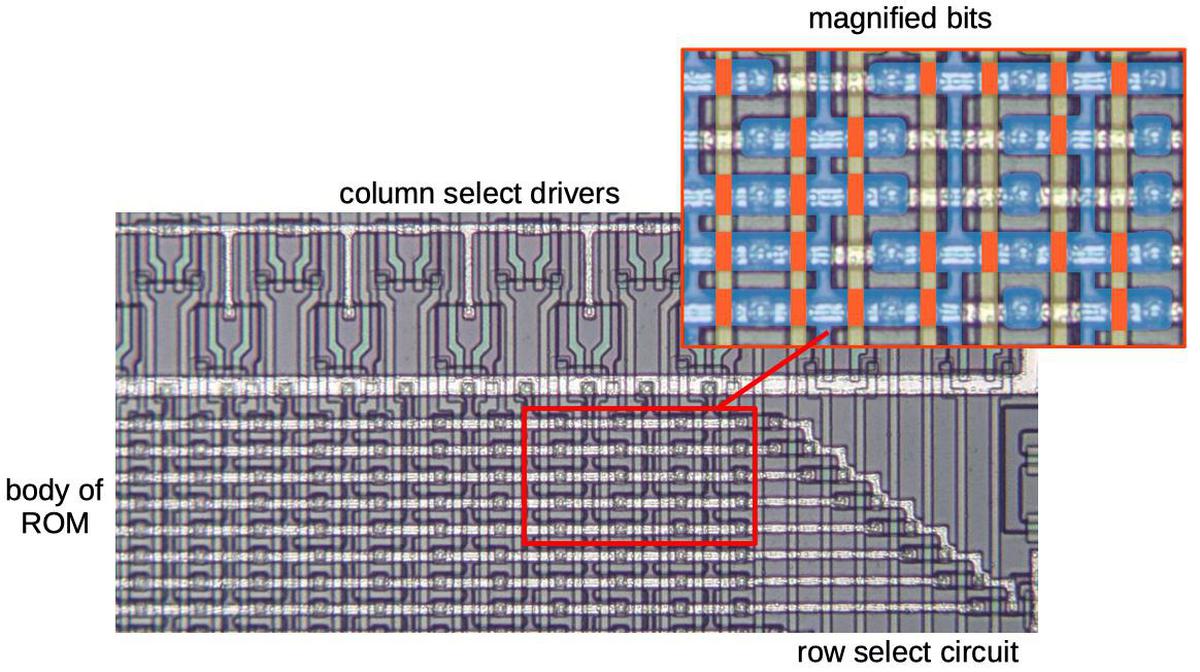
A ROM is arranged in a grid. At each position, silicon is doped to either create a transistor or no transistor, representing a 0 or 1. In a typical ROM, five address bits energize one of 32 vertical select lines to select one column of the ROM. The rows are organized in groups of 8 and three more address bits select one row from each group to yield output bits.
The diagram below shows part of the ROM circuitry. The magnified portion has been colored to show the bits. The vertical column select lines of polysilicon are colored yellow. The ROM is programmed by the pattern of doped silicon (blue). A transistor (red) is formed when a polysilicon line crosses a doped silicon region; the transistors are indicated in red and indicate the bit pattern.
Closeup of the log-sine ROM showing individual bits.
The ROMs use several tricks to reduce space. Duplicate rows are folded together, such as high-order bits that are zero for a range of values. The sine ROM apparently uses delta encoding for alternating values; since the delta values are small, they have a lot of zero bits that can be folded. As a result, the values stored in the ROM are not obvious from the bit patterns. I'm still investigating the ROM representations and will discuss them later.
Adder
Another key building block of the chip is the adder, which sums two binary numbers. The chip has multiple adders: for the phase accumulators, inside the operators, and to apply the envelope.
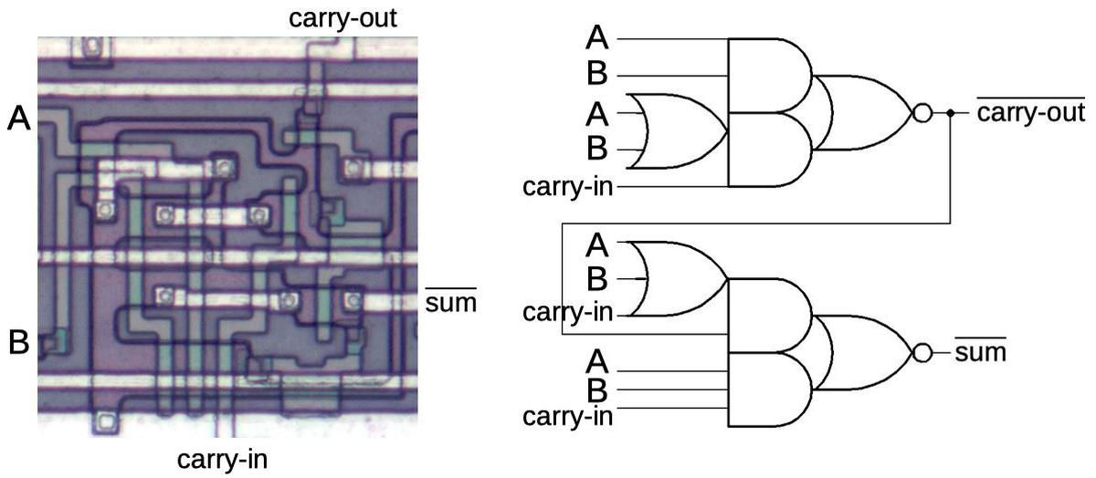
A multi-bit adder is built from full adders, a circuit that adds two bits (along with a carry-in bit), and produces a sum bit (along with a carry-out bit). The diagram below shows how a one-bit full adder is implemented, adding bits A and B along with a carry-in, producing an output sum bit and a carry bit.17Note that the outputs are inverted; other parts of the circuitry deal with that.
Structure of the full-adder circuit used in the chip.
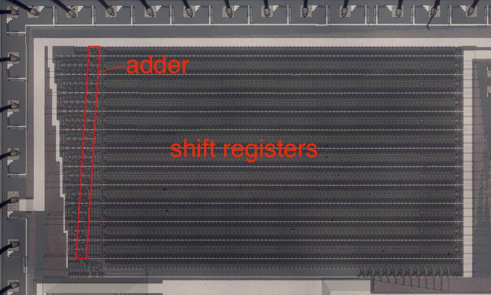
By combining multiple one-bit adders, multi-bit binary numbers can be added as shown in the 23-bit adder below. Note that the adder is at an angle relative to the shift registers. This is a clever trick for performance. One problem with adders is dealing with carries, which may need to propagate through all the bits. (The binary equivalent of needing to repeatedly carry the 1 when computing 999999+1.) The solution is to break the sum into 6 parts. Only 4 bits of each sum are added in each clock phase, so the carry only needs to propagate through 4 bits rather than all 23. The next chunk is added in the next clock phase, and so on.18
The phase adder is at the left of the shift registers that hold the 96 phase values.
Bit shifter
The final building block that I'll discuss is the bit shifter, which shifts a binary value left or right numerically, which is equivalent to multiplying or dividing by a power of 2. A typical shifter is built in two layers: the first layer shifts by 0, 1, 2, or 3 positions. The second layer shifts by 0, 4, 8, or 12 positions. The combination of the two layers permits any shift between 0 and 15 bit positions.
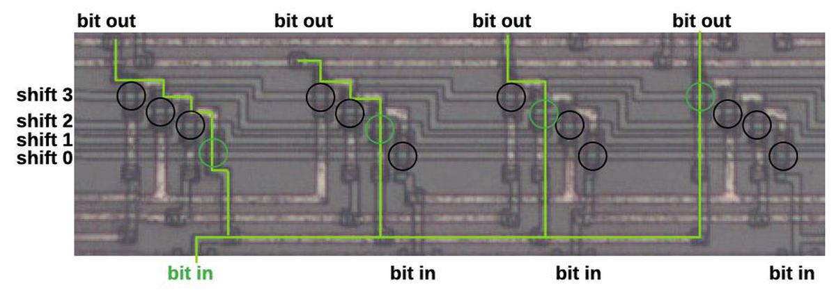
The diagram below shows part of the shifter that shifts by 0, 1, 2, or 3 positions, controlled by the horizontal lines. I've highlighted one of the bits in green. If the "shift 0" line is activated, the leftmost green transistor (circled) will turn on and the green input bit will exit unshifted at the first output position. Likewise, if the "shift 1" line is activated, the second green transistor will turn on and the green bit will exit at the second position, shifted one position to the right. The "shift 2" and "shift 3" lines will cause the green bit to exit two or three positions to the right. The remaining transistors (circled in black) act in the same manner to shift the other bits. The result is that all the bits will pass straight throw (shift 0), or be shifted 1, 2, or 3 positions to the right.
Detail of a shifter circuit.
Shifters are used in combination with the exponential ROMs to compute 2x. The ROM is applied to the fractional part of x, while the shifter is controlled by the integer part. This is much more efficient than using a large ROM to look up the complete value. Another shifter provides a shift of 0 to 6 bits to scale the operator feedback value. A shifter also scales the output value to increase the dynamic range.
Combining and modulating operators with an algorithm
The DX7 generates each note by combining and modulating six operators (oscillators) according to a particular algorithm. This happens sequentially: the chip processes operator 6 for channels 1 through 16, then operator 5 for all the channels, and so forth, ending with operator 1. This cycle of 96 operations repeats, providing new sound values 49096 times a second.19
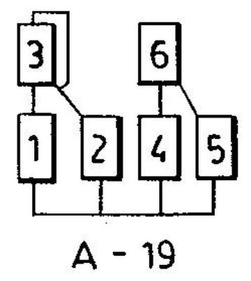
The diagram below shows a typical algorithm. Operator 6 modulates operators 4 and 5, while operator 3 modulates operators 1 and 2, as well as itself. Operators 1, 2, 4, and 5 produce outputs, which are combined to create the final sound value. This section discusses the circuitry that performs the modulations for the specified algorithm.
Algorithm #19 combines the 6 operators in a specific way.
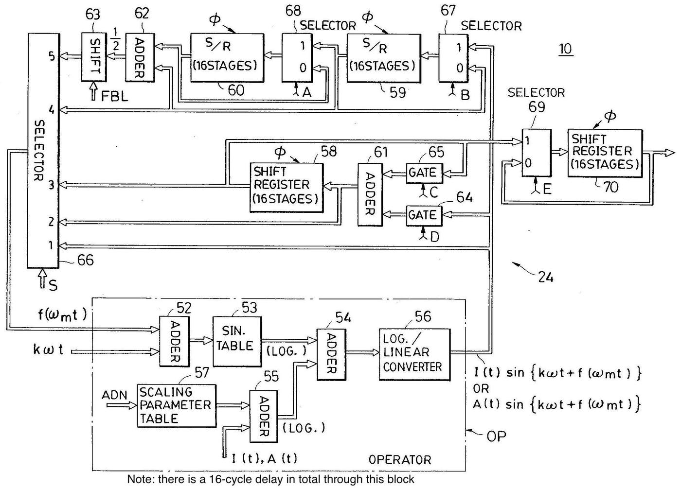
The diagram below shows the implementation of the circuitry to process operators. The lower "operator" box is the circuitry previously discussed: the first adder adds the modulation value f(ωmt) to the current phase value kωt and looks up the value in the sine table. The second and third adders apply the envelope. Finally, the log/linear converter is implemented by the exponential ROM and shifter described earlier.
Diagram showing the construction of an operator, from the patent.
The upper half of the diagram determines the appropriate modulation value f(ωmt) for the selected algorithm and operator. This circuitry is complicated, since there are 5 different cases that the circuitry must handle, chosen by the selector.20The top circuit (selector input 5) implements the feedback of an operator to itself. To provide feedback, the previous two values are stored in 16-stage shift registers, scaled by the feedback level parameter (FBL), and output as the modulation value. (Two previous values are averaged to stabilize the feedback.) Since the 16 channels are processed in sequence, the 16-stage shift registers store the feedback values until the next cycle. The next circuit (selector 4) uses the value of the self-feedback operator to modulate another operator. Selector 3 provides a shift register and adder to sum or delay values. (It is where multiple values are summed to produce the final output.) Selector 2 allows a sum to be used for modulation. Selector 1 is the simple case where the previous operator provides the modulation (e.g. 6 modulating 5). Finally, if no value is selected, the signal remains unmodulated. Control signals A, B, C, D, and E select the specific signal paths.
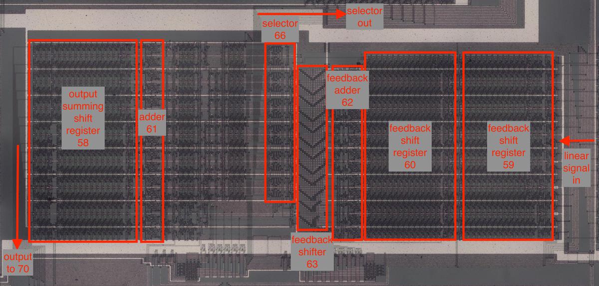
The diagram below shows the implementation of the modulation circuitry on the die. This circuitry corresponds to the upper part of the patent diagram above; the component numbers match the patent numbers. This circuitry occupies the middle portion of the die, with the shift registers taking up the bulk of the space. The adders and feedback level shifter are also visible.
Implementation of the modulation circuitry on the die.
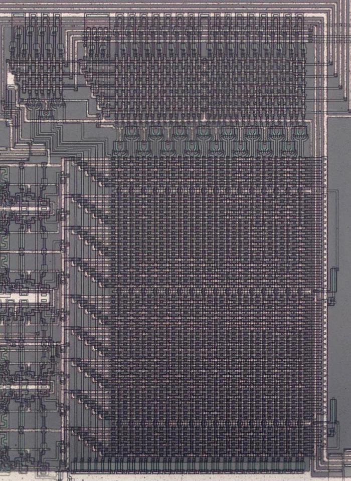
The algorithms are specified by the algorithm ROM (below). This 192×9 ROM produces 9 control signals for the 6 operators in the 32 algorithms. The 16-stage shift register described earlier holds the selected algorithm numbers and provides the input to the ROM. Curiously, it appears that the chip permits each of the 16 notes to use a different algorithm, even though the DX7 does not support this feature.
The algorithm ROM. The circuitry at the top decodes the address (algorithm and operator number), selecting a column from the body of the ROM below. The 9 outputs (A, B, C, D, E, and S) are at the left.
Conclusion
The DX7 was a groundbreaking synthesizer and this chip was at the heart of it, so in a sense this chip was responsible for the 80's sound. Studying the chip's die reveals some interesting circuits. Uncovering the secrets of how the chip operates may help build more accurate DX7 emulators. The chip is complex and this article just scratches the surface so I plan to study the chip in more detail. In particular, I intend to extract the data from the ROMs to find out exactly how the waveforms are represented. In any case, I hope you've found this deep dive into a sound chip interesting.
I announce my latest blog posts on Twitter, so follow me @kenshirriff. I also have an RSS feed. Thanks to Jacques Mattheij and Anthony Richardson for providing the chip and discussion.
