5 storage class memory technology terms you should know (original) (raw)
Memory technologies, such as dynamic RAM, are fast, but they aren't persistent, they have scaling limitations and they're expensive. Storage technologies aren't as fast or as efficient as memory, but they're persistent, can handle large amounts of data and are cheaper.
Storage class memory (SCM) technology, also known as persistent memory, is the next generation of memory and storage technology. It refers to a class of non-volatile memory that aims to close the gap between traditional memory and storage and change the way data is processed and stored.
There are several types of SCM technologies being developed. They retain data and program code when power is lost, and in some cases they log speeds nearly as fast as dynamic RAM (DRAM) and even static RAM (SRAM). This combo of persistence and speed makes it possible to create devices that can be used for both memory and storage.
Storage class memory technology is driving the future of storage and memory. What follows is a look at some of these technologies we're likely to hear a lot more about in the next few years.
3D XPoint
3D XPoint storage class memory technology is already here. Intel and Micron Technology jointly developed this technology to fill the gap in the market between DRAM and NAND flash.
3D XPoint products feature fast performance, ultralow latency and greater endurance than less expensive NAND flash memory. The technology is being used to create some of the fastest SSDs on the market, with low write latency and byte-addressable memory.
[SCM's] combo of persistence and speed makes it possible to create devices that can be used for both memory and storage.
3D XPoint is thought to be a type of resistive RAM (see below), with data storage based on changes in resistance. Its transistorless, cross-point architecture uses electrical current to cause a property change that modifies the cell's resistance level. Each cell holds a single piece of data and represents a 1 or 0, depending on its resistance. 3D XPoint cells can be stacked to improve storage density.
With 3D XPoint architecture, small amounts of data can be written and read, speeding the read/write process and making it more efficient compared with NAND flash memory.
Intel and Micron have said they will end their joint development effort after completing work on the second generation of the technology in the first half of 2019. Micron hasn't shipped any 3D XPoint-based products, but Intel's Optane line of memory and storage products use the technology.

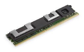
Intel Optane DC persistent memory delivers as much as 36 TB of system-level memory capacity when combined with DRAM.
The Optane memory card comes in an M.2 form factor, with 256 GB, 512 GB and 1 TB capacities. Intel also is shipping Optane DC persistent memory at 128 GB, 256 GB and 512 GB, larger than DRAM, which tops out at 128 GB. Jim Handy, semiconductor analyst at Objective Analysis, has speculated that Optane's density will be a significant benefit, enabling Optane DIMMs to come in at half the price of comparably sized DRAM DIMMs.
Intel's Optane product line also includes several SSDs, including the Optane SSD DC P4800X Series that comes in 375 GB and 750 GB capacities.
Resistive RAM
Another storage class memory technology is resistive RAM, also known as RRAM or ReRAM. It contains a memristor, an electrical component made from a specially formulated dielectric material whose resistance varies depending on the voltage applied. ReRAM is based on resistance switching, which increases the flow of current in one direction and decreases the flow of current in the opposite direction.
Dielectric material, which generally doesn't conduct electric current, will suddenly undergo a dielectric breakdown and conduct a current at high voltages. Conventional dielectric material is permanently damaged by a breakdown. However, in a memristor, the materials used result in a temporary, reversible breakdown.
With one type of memristor, voltage causes microscopic filaments to form in the medium. The application of external voltage causes the filaments to be broken or reversed. The controlled formation and destruction of large numbers of filaments enable data to be stored. Various substances have been tested for this type of memristor, including nickel oxide, titanium dioxide, electrolytes, semiconductor materials and organic compounds.
Another type of memristor uses the voltage to cause nanometal filaments in an amorphous solid called chalcogenide glass. The material is quickly altered from a hardened state to a more fluidlike state, changing its resistance.
Compared with NAND flash, ReRAM offers faster read and write speeds, higher endurance and greater storage density, while consuming less power. Memristor technologies are well suited for memory in industrial and IoT sensors.
Fujitsu and Crossbar are the main vendors offering ReRAM products.
Magnetoresistive RAM
Magnetoresistive RAM, or MRAM, is non-volatile memory that relies on magnetic states to store bits of data as opposed to using electrical charges as DRAM and NAND flash do. MRAM technologies make it possible to deliver speeds much faster than flash and nearly as fast as SRAM, while still retaining data when power is lost.
MRAM uses a pair of ferromagnetic metal plates separated by a thin insulating material layer to determine if a bit is a binary 1 or 0. One plate is permanently magnetized and set to a specific polarity. The other plate's polarity can be switched to match the magnetization of an external memory field. The orientation of the two magnetic fields determines whether a binary bit is a 1 or 0. This MRAM structure is called a magnetic tunnel junction (MTJ). Arrays of MTJs are used in memory devices.
MRAM can perform read and write operations faster than DRAM using less power. Because it's considered to be universal memory, MRAM can be applied to uses ranging from system computing to storage. Unlike flash memory, it doesn't wear out and can be read from and written to until the physical material itself degrades.
Everspin Technologies is the best-known vendor producing this storage class memory technology as stand-alone memory. It originally used a form of MRAM known as Toggle. Everspin has since partnered with GlobalFoundries to produce an embedded version of its MRAM technology that can be integrated into standard CMOS (complementary metal-oxide-semiconductor) technology, replacing embedded flash, DRAM or SRAM. Samsung in March 2019 said it was shipping embedded MRAM as well.
Power use is MRAM's downside. Electrical currents are used to induce the magnetic field in the MTJ to read or write the cell, and that power use is still more than is palatable to enable MRAM to be an ideal DRAM replacement.
Spin-transfer torque MRAM
Spin-transfer torque MRAM (STT-MRAM) is an MRAM variation developed to cut power use. STT-MRAM evaluates the torque applied between the magnetic layers, making more efficient use of the magnetoresistive properties.
STT-MRAM is based on a perpendicular MTJ and the concept that electrons have angular momentum or spin. Spin and orbital are the two types of angular momentum in quantum mechanics. Using electric current through a magnetic field, STT-MRAM changes the electron spin to an up or down state. The spin in the electron flow from one MTJ plate to the other can change the magnetic orientation on the second plate.
An MTJ that uses STT draws less power than MRAM's electrically induced MTJ. STT-MRAM also can be made smaller than MRAM, enabling greater memory density in devices. However, for high-speed performance, STT-MRAM still uses too much power to enable it to be economically viable as a DRAM replacement.
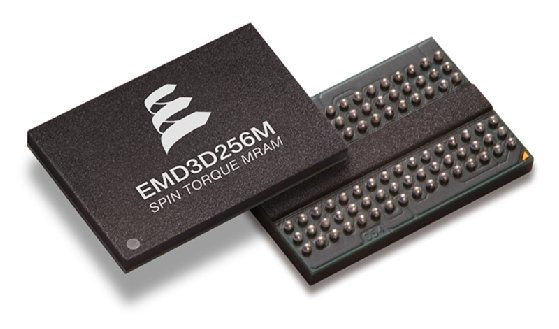
Everspin offers a 256 Mb STT-MRAM device. It also has a line of STT-MRAM-based storage accelerator SSDs that deliver speeds close to DRAM with 1 GB capacity.

Everspin ST-DDR3 STT-MRAM is designed for applications such as SSD buffers, RAID buffers or synchronous logging.
Nanotube RAM
Nanotube RAM, or NRAM, is proprietary storage class memory technology developed by Nantero. It's made up of carbon nanotubes, which Nantero describes as 1/50,000 the size of the diameter of a human hair but 50 times stronger than steel, half as dense as aluminum and having thermal and electrical conductivity properties better than any material known to science.
An NRAM cell is made up of a film of interlinked carbon nanotubes layered on a silicon substrate. The nanotube layer sits between two electrodes and can be electrically compressed or expanded so the nanotubes are touching each other or slightly separated to create a high or low state of resistance. When the nanotubes aren't in contact with one another, the resistance is high and represents a 0 state. When they're touching, they're held in place by van der Waals forces, and the resistance of the fabric is low, representing a 1 state.
Nantero says its NRAM is as fast as and denser than DRAM, uses no power in standby mode, has 160 times less write energy per bit than flash and is highly resistant to environmental issues, such as extreme temperature.
The semiconductor products Nantero has developed use NRAM on existing CMOS fabs, so no new equipment or processes are required. Only a small number of process steps and one mask layer are required for fabrication, keeping costs low, Nantero says, and it's compatible with 3D architectures and multi-level cell operation.
Nantero said in 2018 it was developing a multi-Gb, DDR4-compatible, non-volatile, stand-alone memory product, a stand-alone chip designed as an SSD or HDD cache with embedded memory offerings for automotive and IoT applications. Two Fujitsu semiconductor businesses have licensed Nantero NRAM technology and are expected to bring products to market in 2019.