Simple Dual Port RAM System - Simple dual-port RAM that supports simultaneous read and write
operations - Simulink ([original](https://www.mathworks.com/help/hdlcoder/ref/simpledualportramsystem.html)) ([raw](?raw))Simple dual-port RAM that supports simultaneous read and write operations
Libraries:
HDL Coder / HDL RAMs
Description
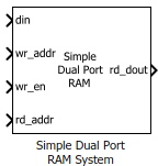
The Simple Dual Port RAM System block models a simple dual-port RAM that supports simultaneous read and write operations through a single output port for read data. To configure this block, open the block and set the Type of RAM to Simple dual port. By using this block, you can:
- Create parallel RAM banks by using vector data at thedin, addr, andwe ports.
- Specify an initial value for the RAM using the Initial output of RAM parameter.
- Perform asynchronous read in target hardware by selecting theUse asynchronous read feature in target hardware parameter.
- Perform cycle-accurate read operation by selecting the Model RAM with one cycle of delay parameter.
- Use the column-write method to write to specified bits in an addressed memory location.
Note
During a write operation, if a read operation occurs simultaneously at the same address, old data appears at the read output port.
Limitations
- When you build the FPGA bitstream for the RAM, the global reset logic does not reset the RAM contents. To reset the RAM, implement the reset logic.
- The RAM address can be either
fixed-point (fi)orinteger, must be unsigned, and must be between2and31bits long.
Ports
Input
Data to write, specified as a scalar or a vector. You can write the data into the RAM memory location when the write enable signal at portwe is true. This value can be an integer, or of type double,single or half. The value can also be a fi object and can be real or complex.
Bus Support:
You can use non-virtual bus and arrays of buses for HDL code generation.
Data Types: single | double | half | int8 | int16 | uint8 | uint16 | Boolean | fixed point
Address to write, specified as a scalar or a vector. Use this address to write to RAM when the signal at port we istrue. This value can be either afixed-point (fi) or an unsignedinteger and must be between 2 and 31 bits long.
Data Types: uint8 | uint16 | fixed point
Write enable, specified as a scalar or a vector. When the signal at port we is true, the block writes the data into the specified memory location. When the signal at port we is false, the block reads the value from the memory location specified byrd_addr port.
Note
To use column-write method, the data type must be aninteger or afixed-point.
Data Types: uint8 | uint16 | uint32 | uint64 | Boolean | fixed point
Address to read, specified as a scalar or a vector. Use this address to read from the RAM. This value can be either a fixed-point (fi) or an unsigned integer and must be between 2 and 31 bits long.
Dependencies
To enable this port, set the Type of RAM parameter to Simple dual port orDual port.
Data Types: uint8 | uint16 | fixed point
Output
Read output data, returned as a scalar or vector. The RAM reads the old output data from the memory location specified byrd_addr port.
Parameters
Main
Type of RAM, specified as either:
Single port— Create a single port RAM with write data, address, and write enable data as inputs and read data as the output.Simple dual port— Create a simple dual port RAM with write data, write address, write enable, and read address as inputs, and data from the read address as the output.Dual port— Create a dual port RAM with write data, write address, write enable, and read address as inputs, and data from the read address and write address as the outputs.True dual port— Create a true dual port RAM with write dataaandb, write and read addresses foraandb, and write enableaandbas inputs and data from write addressesaandbas the outputs.Simple tri port— Create a simple tri port RAM with write data, write address, write enable, and read addressesaandbas inputs and data from read addressesaandbas the outputs.
The code generator dynamically configures the input and output ports of the block based on the RAM type that you specify.
Programmatic Use
| **Block Parameter:**RAMType | |||
|---|---|---|---|
| Type: character vector, string | |||
| Values: Dual port | Simple dual port | Single port | True dual port | Simple tri port |
| Default: Simple dual port |
Enable this option to allow the hardware to execute a read instruction immediately, without waiting one cycle.
Programmatic Use
| **Block Parameter:**AsyncRead |
|---|
| Type: character vector, string |
| Values: 'on' | 'off' |
| Default: 'off' |
Specify the initial simulation output of the RAM by using one of these options:
- A scalar value.
- A vector with a one-to-one mapping between the initial value and the RAM words.
- An n_-by-m matrix with a one-to-one mapping between the initial values and the RAM words in the RAM banks, where_n represents the number of RAM banks and m represents the number of address locations in the RAM block, or vice-versa.
Programmatic Use
| **Block Parameter:**RAMInitialValue | |
|---|---|
| Type: integer, floating point | |
| Values: 0.0 | Scalar | Vector |
| Default: 0.0 |
Data Types: single | double | int8 | int16 | int32 | int64 | uint8 | uint16 | uint32 | uint64
Advanced
Since R2024b
- When you select this parameter, the RAM delays the input data by one cycle before the output can read it. Use this option to ensure the block is cycle-accurate with the generated HDL code.
- When you clear this parameter, the RAM reads and outputs the input data immediately, but adds one cycle of latency during HDL code generation. Use this option to leverage clock-rate pipelining when you specify an oversampling value or work with multirate models.
Dependencies
To enable this parameter, clear the Use asynchronous read feature in target hardware parameter.
Programmatic Use
| **Block Parameter:**ModelRAMDelay |
|---|
| Type: character vector, string |
| Values: 'on' | 'off' |
| Default: 'on' |
Since R2025a
- When you set this parameter to
serial, the code generator infers parallel banks of RAM from vector inputs to RAM System block. - When you set this parameter to
parallel:- The code generator does not scale up RAM consumption with the size of the vector input when you generate HDL Code. Instead, it applies each operation of the input signals one at a time, starting with the first index. Enabling serial access allows you to leverage multicycle RAM access at a faster clock rate while modeling with a vector input at the data rate.
- If the RAM System block exists in a clock-rate pipelining region, the serialization uses a clock-rate implementation instead of local multirate implementation.
Dependencies
To enable this parameter, clear the Model RAM with one cycle of delay parameter or enable the Use asynchronous read feature in target hardware parameter.
Programmatic Use
| **Block Parameter:**VectorAccess |
|---|
| Type: character vector, string |
| Values: 'serial' | 'parallel' |
| Default: 'serial' |
More About
You can use the column-write method to view the RAM as a collection of equally sized columns. During a write cycle, you can write into each of these columns separately. The data type and value of the write enable input, along with the data type of write data input, determine the size of each column and the columns in which the block writes in the addressed memory location.
In this context:
- DT is the data type of the write data input signal
din. - DW is the data width of the input data, which is equal to word length of the
dinvalue. - DTWE is the data type of the write enable signal
we. This signal determines which columns the block writes in the addressed memory location. The block writes the columns based on the position of the 1s in the binary representation of the value ofwe. - NC is the number of columns which you can partition the RAM space to write the data, which is equal to word length of
wevalue. - WC is the width of each column, which is equal to_DW_ divided by NC.
The table summarizes the relationship among the data types of the write data input, the data types of write enable input, the number of columns, and the width of each column.
| DT | DW | DTWE | NC | WC in Bits |
|---|---|---|---|---|
| uint16 | 16 | ufix4 | 4 | 4 |
| uint32 | 32 | ufix4 | 4 | 8 |
| uint64 | 64 | ufix4 | 4 | 16 |
| uint32 | 32 | uint8 | 8 | 4 |
| uint64 | 64 | uint8 | 8 | 8 |
| int32 | 32 | uint16 | 16 | 2 |
For example, if DT is uint16 and_WE_ is ufix4, then DW is equal to 16, NC is equal to 4, and WC is equal to 4 bits. If the input to din is 980, its binary representation is 0000001111010100. The column-wise representation of din is c4 = 0000, c3 =0011, c2 = 1101, and c1 =0100, where c1 is the first column.
The table summarizes the results of using the column-write method for different input combinations.
| Value of we | Binary Representation ofwe | Columns Selected for Writing in RAM | Data at Memory Location | dout | |
|---|---|---|---|---|---|
| Before Performing Write Operation | After Performing Write Operation | ||||
| 3 | 0011 | c2, c1 | c4 = 0000c3 =0000 c2 =0000c1 =0000 | c4 = 0000c3 =0000c2 =1101c1 =0100 | 212 |
| 4 | 0100 | c3 | c4 = 0000c3 =0000c2 =0000c1 =0000 | c4 = 0000c3 =0011 c2 = 0000c1 =0000 | 768 |
| 6 | 0110 | c3, c2 | c4 = 0000c3 =0000c2 =0000c1 =0000 | c4 = 0000c3 =0011c2 =1101c1 =0000 | 976 |
| 9 | 1001 | c4, c1 | c4 = 0000c3 =0000c2 =0000c1 =0000 | c4 = 0000c3 =0000c2 =0000c1 =0100 | 4 |
| 9 | 1001 | c4, c1 | c4 = 1111c3 =1111c2 =1111c1 =1111 | c4 = 0000c3 =1111c2 =1111c1 =0100 | 4084 |
Limitations
- Inputs with signed data types and with non-zero fraction lengths are not supported by the write enable input port.
- The word length of the write data input must a multiple of the word length of the write enable.
Extended Capabilities
HDL Coder™ provides additional configuration options that affect HDL implementation and synthesized logic.
HDL Architecture
The block has a MATLABSystem architecture which indicates that the block implementation uses the hdl.RAM System object™.
HDL Block Properties
| General | |
|---|---|
| ConstrainedOutputPipeline | Number of registers to place at the outputs by moving existing delays within your design. Distributed pipelining does not redistribute these registers. The default is0. For more details, see ConstrainedOutputPipeline. |
| InputPipeline | Number of input pipeline stages to insert in the generated code. Distributed pipelining and constrained output pipelining can move these registers. The default is0. For more details, see InputPipeline. |
| OutputPipeline | Number of output pipeline stages to insert in the generated code. Distributed pipelining and constrained output pipelining can move these registers. The default is0. For more details, see OutputPipeline. |
| RAMDirective | Specify whether to map RAM blocks in your design to RAM blocks on the target FPGA. For UltraRAM mapping,Initial output of RAM must be set to 0. For more details, see RAMDirective. |
Complex Data Support
This block supports code generation for complex signals.
Restrictions
The block does not support:
- Nested bus at the data port.
- Non-zero values at the Initial output of RAM when using non-virtual bus input to the data port.
Version History
Introduced in R2017b
You can use Simple Dual Port RAM System block inside a data rate feedback loop and use clock-rate pipelining optimization. This model design is helpful for applications that require programmable or tunable lookup tables without having to regenerate bitstreams.
Use the new parameter Model RAM with one cycle of delay to model delay in your simulation. Model RAM with one cycle of delay is enabled by default and is disabled when Use asynchronous read feature in target hardware is enabled.
These parameters are renamed:
| Previous Name | Current Name |
|---|---|
| Specify the type of RAM | Type of RAM |
| Enable asynchronous reads | Use asynchronous read feature in target hardware |
| Specify the RAM initial value | Initial output of RAM |
In this block, you can use the column-write method to selectively modify specific parts of the memory without altering the remaining parts at a specified memory address.
In this block, you can initialize RAM banks with unique initial values.
The block now supports HDL code generation for input data specified as an array of buses.
The block now supports HDL code generation with input data of typeHalf orBoolean.
See Also
Objects
Blocks
- Dual Port RAM System | Single Port RAM System | True Dual Port RAM System | Simple Tri Port RAM System