FPGA Targeting Workflow - MATLAB & Simulink (original) (raw)
You can use the hardware-software (HW/SW) co-design workflow of the SoC Blockset™ Support Package for AMD FPGA and SoC Devices to target only the FPGA fabric of the underlying Zynq® system on chip (SoC). FPGA targeting uses code generation that translates a designated subsystem to HDL code and creates a custom bitstream for the FPGA fabric. This custom bitstream is then downloaded to the FPGA on the development board. By moving part or all of your algorithm to the hardware, you speed up host processing. You can also use FPGA targeting for prototyping designs on real hardware. FPGA targeting support is available for both the receive path and the transmit path, one at a time.
Limitations
- Duplex operation using both Transmitter and Receiver blocks in the same model occurs only when targeting the ARM® processor using the full HW/SW co-design workflow. It is recommended to do either transmit or receive FPGA targeting, but not both.
- Transmitter FPGA targeting and receiver FPGA targeting do not support resource sharing.
Before You Begin
To target only the FPGA fabric of the Zynq SoC, you must install HDL Coder™ and the HDL Coder Support Package for AMD FPGA and SoC Devices.
In addition, you must install the following third-party tools:
- Xilinx® Vivado® development tools, version 2024.1
To install all required software products, follow the steps outlined in Installation for Hardware-Software Co-Design (skip step 4).
Step 1. Create an Algorithm
When designing an SDR algorithm for the Zynq radio hardware, each Receiver and Transmitter block of your design must meet the following Simulink® requirements:
Number of Channels
The number of channels varies between the supported RF cards.
- ADI RF SOM — both one and two channels are supported. If you are using a single channel, use a single channel data source. If you are using both channels, use a double channel data source.
- ADI FMCOMMS2 or FMCOMMS3 — both one and two channels are supported. If you are using a single channel, use a single channel data source. If you are using both channels, use a double channel data source.
- ADI FMCOMMS4 — one channel. Use a single channel data source.
- ADI FMCOMMS5 — four channels are supported. If you are using a single channel, use a single channel data source. If you are using multiple channels, use a multiple channel data source.
Input/Output Signal Guidelines
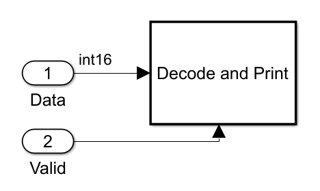
The workflow has specific requirements for the boundary of the user logic subsystem. The following diagram shows the data and valid user logic inputs and outputs for a single-channel user logic subsystem. Multiple-channel reference designs contain multiple sets of I and Q data lines.
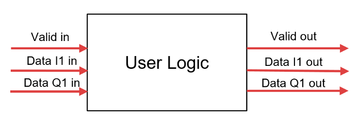
- Each data input or output must be 16 bits. Complex inputs and outputs are not supported at the ports of the HDL subsystem. Therefore, real and imaginary signals must be modeled at the subsystem boundaries.
- Model all of the ports for a given reference design, even when the ports are not used.
- The data inputs and outputs to the subsystem are modeled using separate data and valid signals. In Simulink, the data and valid lines must be driven at the same sample rate. Therefore, the input and output clock rates of the subsystem must be equal.
- Clock the data and valid signals at the fastest rate of the HDL subsystem.
- When the Tx data valid out signal is de-asserted, the last sample value is held.
- When the Rx data valid out signal is de-asserted, the associated sample is not sent back to the host. If you have a large downsampling factor within your receiver user logic, the host receive block is at risk of timing out.
Scalar Mode
For HDL code generation, your custom algorithm must operate in scalar mode. You can convert frame-based input signals to the scalar data type by using theUnbuffer block. You can then convert the output back to frame signals using the Buffer block. Within this boundary ofUnbuffer and Buffer blocks, the algorithm operates in scalar mode, which is necessary for HDL code generation.
Step 2. Verify Radio Hardware Connection
Before you can target the FPGA, the host computer must be communicating with the radio hardware.
- Create a radio object with the
sdrdevfunction. If you are using an FMCOMMS5 radio hardware, specify'FMCOMMS5'instead of'AD936x'when callingsdrdev.
radio = sdrdev('AD936x'); - Verify host-radio communication by calling the
testConnectionmethod on the radio object.
This function queries the device and returns either success or failure.
Step 3. Set Up Third-Party Tools
Set up your system environment to access Xilinx Vivado from MATLAB®. The hdlsetuptoolpath function adds the required folders to the MATLAB search path, using the Xilinx installation folder that you specify.
For example:
- In Windows®:
hdlsetuptoolpath('ToolName','Xilinx Vivado','ToolPath', ...
'C:\Xilinx\Vivado\2024.1\bin\vivado.bat') - In Linux®:
hdlsetuptoolpath('ToolName','Xilinx Vivado','ToolPath', ...
'/opt/Xilinx/Vivado/2024.1/bin')
Step 4. Generate HDL IP Core Using HDL Workflow Advisor
HDL IP core generation enables you to generate a shareable and reusable IP core module from a Simulink model automatically. HDL Coder generates HDL code from the Simulink blocks. By using an SDR reference design, you can create an IP core that integrates into the radio hardware.
After you are satisfied with the simulation behavior of the hardware subsystem, generate the HDL IP core and integrate it with the SDR reference design.
Setup
- Make sure that the HDL subsystem is treated as an atomic unit. You can check this setting by right-clicking the subsystem that contains the algorithm and selecting Block Parameters (Subsystem).
- Start the HDL Workflow Advisor by right-clicking the subsystem that contains the algorithm and selecting > .
A. Set Target
- At Workflow Advisor Step 1.1, select
IP Core Generationfor the Target workflow.Then select the required Zynq radio hardware for the Target platform.- ADI RF SOM
- ZedBoard and FMCOMMS2/3/4
- ZC706 and FMCOMMS2/3/4
- ZC706 and FMCOMMS5
- ZCU102 and FMCOMMS2/3/4
Finally, selectXilinx Vivadoas theSynthesis tool. Accept the default Project folder, or enter a valid path for the location of your project folder. All other fields are populated automatically.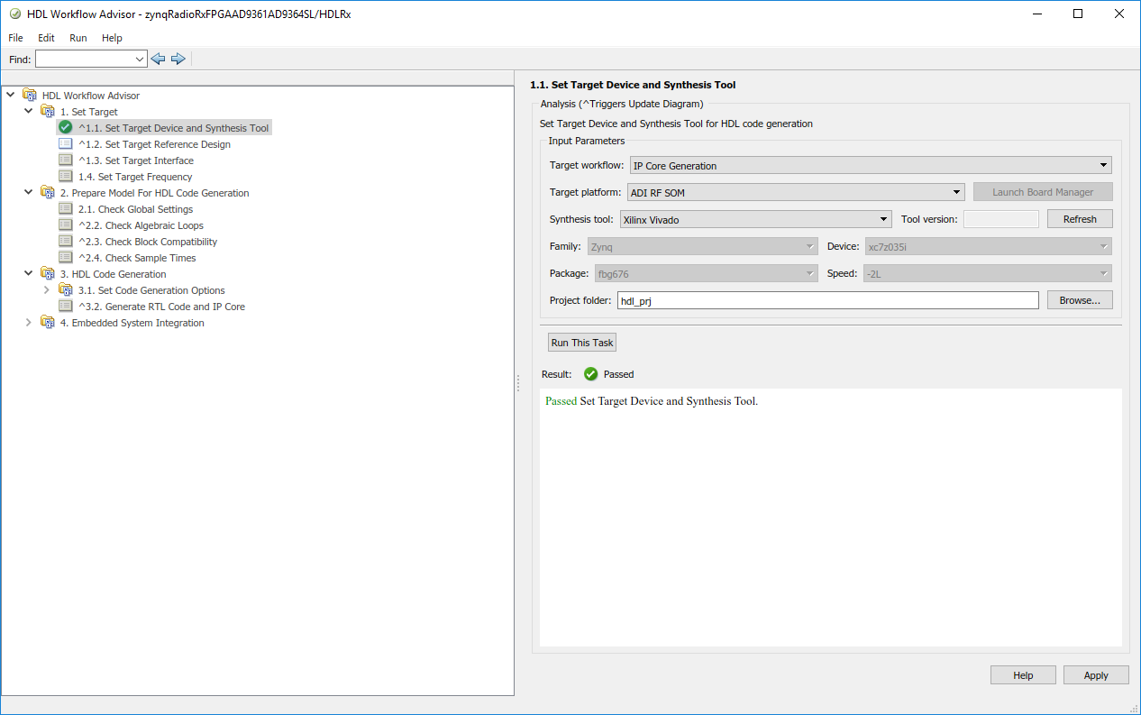
Click Run This Task.
- At Workflow Advisor Step 1.2, select the reference design for your system. Select only one of these options:
Receive pathTransmit path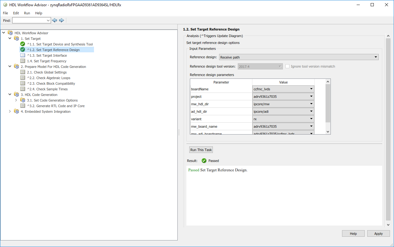
Click Apply, and then click Run This Task. Check for warnings in the log text area at the bottom of the Workflow Advisor and make the required changes before proceeding.
- At Workflow Advisor Step 1.3, set the target interface and verify thatProcessor/FPGA synchronization is set to
Free running. Then map your user logic to the reference design. When mapping the RF channels, each I and Q component refers to a 16-bit port on the user logic. The number defines the channel designation. For example,Baseband Rx I1 In [0:15]maps to the real part of the receiver for channel 1 on the RF card. Ensure that the appropriate target platform interfaces are selected for each port.
Click Apply, and then click Run This Task. - At Workflow Advisor Step 1.4, choose the target frequency for your design.
Click Run This Task.
B. Run Design Checks
In Workflow Advisor Step 2, click Run All to check and prepare your design for HDL code generation. If any task fails or warns, try to correct the issue. You cannot continue until you resolve all issues.
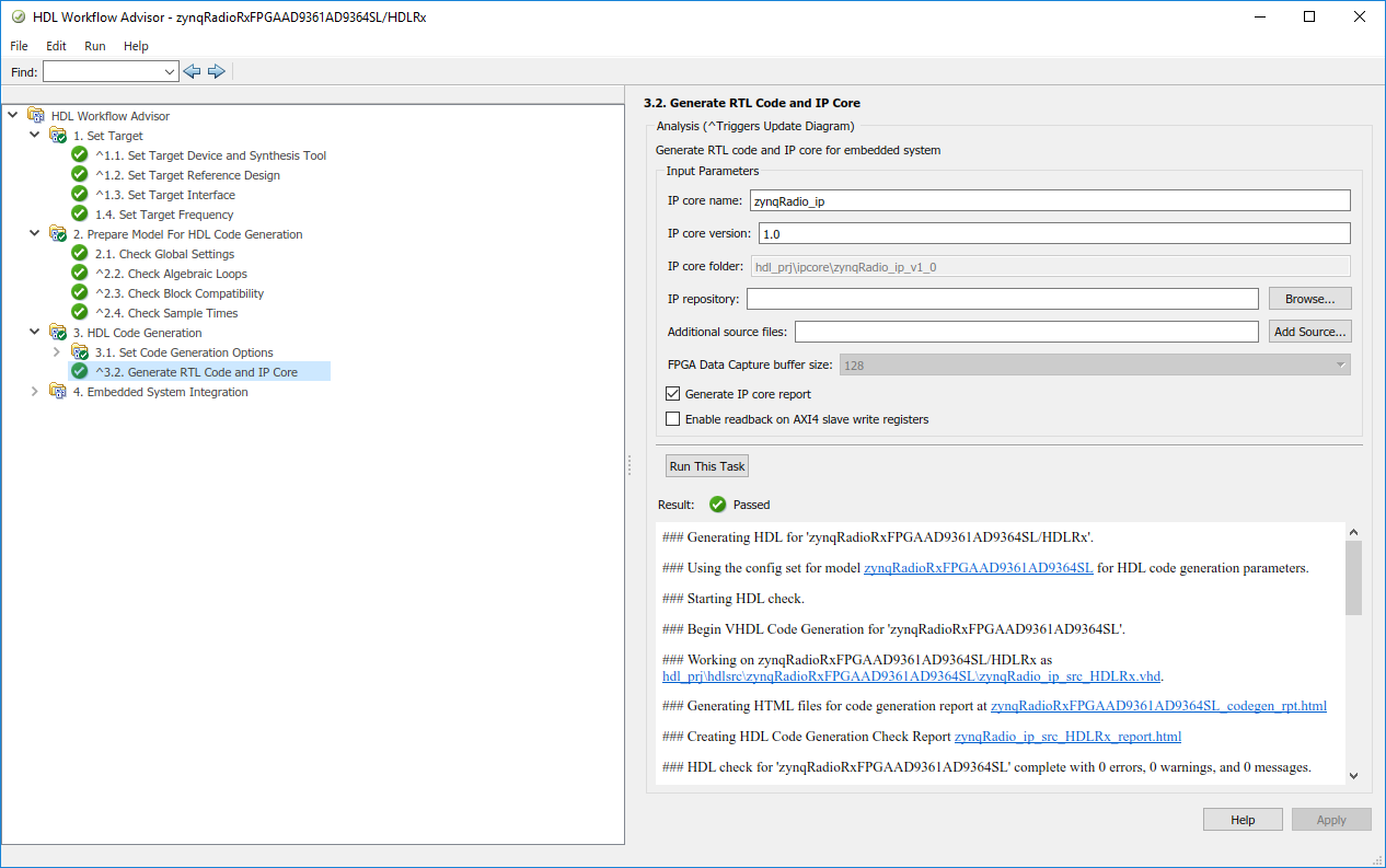
C. HDL Code Generation
In Workflow Advisor Step 3, click Run All to generate HDL code for the IP core.
D. Embedded System Integration
- Workflow Advisor Step 4.1 integrates the IP core into the SDR reference design and generates a Vivado project. To create the project, set Synthesis objective to
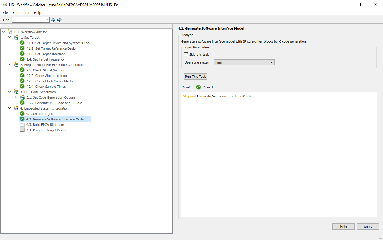
None, and clickRun This Task. - Workflow Advisor Step 4.2 is needed only in the Hardware-Software Co-Design Workflow, when targeting both the ARM processor and the FPGA fabric. Select Skip this task, and then click Run This Task.
- Workflow Advisor Step 4.3 generates a bitstream for the FPGA fabric. To generate the bitstream in an external shell, select
Run build process externally. With this option, you can keep using MATLAB while the FPGA image builds. Click Run This Task. The step completes in several minutes, after basic project checks have been performed, and the step is marked with a green check mark. Before continuing, verify in the external command window that the Vivado bitstream built without printing an error. - Program the Zynq hardware.
Workflow Advisor Step 4.4 downloads the bitstream onto the device.
Before continuing with this step, call thezynqfunction with the following syntax to make sure that MATLAB is set up with the correct physical IP address of the radio hardware.
devzynq = zynq('linux','192.168.3.2','root','root','/tmp');
By default, the physical IP address of the radio hardware is 192.168.3.2. If you alter the radio hardware IP address during the hardware setup process, you must supply that address instead.
In Workflow Advisor Step 4.4, you have three options to download the bitstream.- With
Download, the bitstream is persistent across power cycles (recommended). - With
JTAG, the bitstream is not persistent across power cycles
Alternatively, if you want to load the bitstream outside Workflow Advisor, call thedownloadImagefunction. If you are using and FMCOMMS5 radio hardware, specify'FMCOMMS5'instead of'AD936x'when callingsdrdev.
radio = sdrdev('AD936x');
downloadImage(radio,'FPGAImage',...
'hdl_prj\vivado_ip_prj\vivado_prj.runs\impl_1\system_top.bit')
This function call renames the generatedsystem_top.bitfile tosystem.bitand downloads the file over an Ethernet connection to the radio hardware. This bitstream is persistent across power cycles.
- With
Step 5. Verify Hardware Implementation
A. Replace Subsystem
Create a separate model to test and verify the targeted subsystem. Use the original components and replace the subsystem used to generate the custom bitstream with I/Os to the radio hardware.
The following example shows this process for the HDLRx subsystem.
Receiver with HDLRx Subsystem

In the following retargeted HDL-optimized receiver model, the HDLRx subsystem is removed. The retargeted model contains only the decoding components from the original model. The components that made up the HDLRx subsystem are now implemented on the FPGA.
Retargeted Model
B. Run Simulation
Run the simulation. The model now produces real-time data from your algorithm output.
See Also
Functions
- sdrdev | hdlsetuptoolpath (HDL Coder) | zynq (Embedded Coder)