photonic integrated circuits (original) (raw)
Acronym: PIC or PLC = planar lightwave circuit
Definition: integrated circuits with optical functions
Alternative term: planar lightwave circuits
Categories:  photonic devices,
  optoelectronics,
  lightwave communications
- photonic integrated circuits
- quantum photonic integrated circuits
Related: integrated opticssilicon photonicsoptoelectronicsoptical fiber communicationsfiber to the homequantum information processing
Page views in 12 months: 2780
DOI: 10.61835/9kc Cite the article: BibTex BibLaTex plain textHTML Link to this page! LinkedIn
Content quality and neutrality are maintained according to our editorial policy.
📦 For purchasing photonic integrated circuits, use the RP Photonics Buyer's Guide — an expert-curated directory for finding all relevant suppliers, which also offers advanced purchasing assistance.
Contents
What are Photonic Integrated Circuits?
Quantum Photonic Integrated Circuits
Packaging of Photonic Integrated Circuits
Summary:
This article provides a comprehensive overview of photonic integrated circuits (PICs), which are chip-scale devices integrating multiple optical components on a single substrate. It details the various material platforms used for fabrication, including silicon photonics, indium phosphide (InP), silicon nitride, and lithium niobate, comparing their respective advantages like mode confinement, propagation loss, and component implementability.
The text also explores the growing complexity of PICs, their crucial role in emerging fields like quantum photonics, and significant challenges in packaging and manufacturing. Finally, it discusses key application areas such as optical communications, sensing, and quantum computing, as well as the foundry model for PIC production.
(This summary was generated with AI based on the article content and has been reviewed by the article’s author.)
What are Photonic Integrated Circuits?
A photonic integrated circuit (PIC) — also called a planar lightwave circuit (PLC) or an integrated optoelectronic device — is a chip-scale device in which multiple optical (and often also electronic) components are integrated onto a single substrate. Analogous to electronic integrated circuits for electrons, PICs manipulate and process light signals in compact, scalable formats.
PICs typically include a combination of passive components (waveguides, couplers, optical filters, splitters, resonators) and active components (lasers, modulators, amplifiers, photodetectors). The field of research and technology enabling such devices is called integrated optics.
Fabrication is generally carried out using wafer-scale micro- and nanofabrication techniques such as lithography, etching, and thin-film deposition. Various substrate materials can be used, each with characteristic benefits and limitations. The most common include silicon, fused silica (silica glass), indium phosphide (InP), silicon nitride (Si₃N₄), and lithium niobate (LiNbO₃).
Used Substrate Materials
The choice of substrate material determines many properties of a PIC platform, such as transparency window, mode confinement, achievable component types, and fabrication cost. In the following sections, the most important platforms are explained.
Fused Silica (SiO2)
Waveguides can be fabricated in fused silica by dopant diffusion, UV photolithography, or by ultrafast-laser micromachining. The low propagation losses of silica make it attractive for passive components like splitters, filters, and large waveguide arrays. Rare-earth doping enables optical amplifiers and lasers. As the refractive index contrast is quite low, effective mode areas are relatively large. Although this makes coupling to fibers easier, it also implies high bend sensitivity, thus stringent limits on bend radii, which leads to relatively large circuit footprints.
Silica on Silicon
By layering silica films on silicon wafers, one can use methods of standard microelectronics fabrication. These waveguides form the basis of many components in wavelength division multiplexing (WDM), such as multiplexers/demultiplexers, Mach–Zehnder interferometers and arrayed waveguide gratings (AWGs). Silica-on-silicon is thus widely used in commercial fiber optic communications. Coupling to fibers and fiber arrays is relatively easy.
Silicon Photonics (Si)
Silicon photonics is a rapidly developing platform that integrates photonic functions directly on silicon chips. The strong refractive index contrast yields tight optical confinement, enabling small bend radii and dense integration of optical components.
Silicon photonics is highly compatible with CMOS fabrication, allowing co-integration with electronics.
However, as silicon has an indirect band gap, it is not suitable for efficiently generating light; lasers usually require hybrid integration with InP or other III–V semiconductors.
Indium Phosphide (InP)
Being a direct-bandgap compound semiconductor, InP is the basis for PICs which can integrate lasers, amplifiers, modulators, and detectors. This platform underpins high-performance optical fiber communication systems. Fabrication is more costly than silicon, but it allows the greatest degree of “all-in-one” integration.
Silicon Nitride (Si3N4)
Silicon nitride is an emerging platform which is valued for its broad transparency window (from visible to mid-IR), very low propagation losses, and suitability for high-Q optical resonators, apart from couplers, filters, arrayed waveguide gratings and others. It combines moderate refractive index contrast with excellent fabrication maturity, enabling applications in nonlinear photonics, sensors, and precision frequency comb sources.
Lithium Niobate (LiNbO3)
Lithium niobate is a ferroelectric crystal material with strong ($\chi^{(3)}$) nonlinearity as well as strong electro-optic and acousto-optic effects. Waveguides can be fabricated on lithium niobate substrates e.g. via proton exchange or by indiffusion of titanium, in any case controlled by a lithographic method. The birefringence of this material is both a useful tool (for polarization control) and a challenge: Polarization-independent designs are difficult, which is a problem for optical fiber communications.
Lithium niobate PICs support high-speed, high-linearity modulators and efficient nonlinear frequency conversion devices.
Comparing PIC Platforms
A wide range of important properties needs to be considered when comparing PIC platforms. In particular:
- Transparency window: This is obviously essential for many applications, requiring certain operating wavelengths.
- Mode confinement, governed by the refractive index contrast, is strong for some technologies like silicon but much weaker for others like silica. Strong mode confinement means small effective mode area and loss sensitivity for bend losses, allowing for tightly bent waveguides. That enables a high density of components.
- Propagation losses vary a lot, and can also depend substantially on operation wavelengths. They are particularly important for quantum PICs, but also in other applications, e.g. requiring high-Q optical resonators. Particularly low losses are possible for Si3N4.
- Note that platforms allowing small devices due to strong confinement, allowing tightly bent waveguides, are less sensitive to losses.
- Polarization properties can have important implications. Some materials like silica allow for non-birefringent waveguides, while for others (e.g. LiNbO3) birefringence is unavoidable. In some cases, birefringence is useful.
- The coupling efficiency to fibers or free space can also be important. A strong mismatch of mode sizes is generally detrimental, although there are mode size adapter technologies which can cope with that problem.
- Device implementability: Certain types of components are easily implemented in some platforms, while difficult in others. For example, LiNbO3 is particularly suitable for electro-optics and nonlinear frequency conversion, which is difficult or impossible in silica. For some application areas, this more or less excludes certain platforms, or requires hybrid approaches. Possible device performance, such as modulator bandwidth, can also vary.
- Quantum PICs have special requirements concerning needed components, and often cryogenic operation.
- Compatibility with CMOS technology, for example, is relevant in some areas, where one needs to co-integrate with electronics using mature CMOS foundry techniques. Silicon photonics technology is outstanding in this respect.
- Thermal properties can be relevant for densely integrated devices. Materials differ both in thermal conductivity and sensitivity.
- Manufacturing cost (considering required equipment and processing cost) can substantially depend on the PIC platform, but also on the required types and complexity of functions.
- Scalability of the platform, i.e., the suitability also for complex circuits, depends on component density, the possibility to process large substrates, and the device yield.
As so many aspects are relevant, the choice of a PIC platform can be far from obvious. In many cases, no platform is ideal in all respects, and compromises are unavoidable. One may also need to take a hybrid approach, combining two platforms, which introduces additional complications.
Predicting the future importance of specific PIC technologies is also difficult. This depends on the technological progress (driven by substantial investments), but also on the demands of various technology areas. For example, quantum PICs may become very important, depending on the general advances of quantum technologies.
Circuit Complexity
PICs can host anything from simple two‑component waveguide devices to highly integrated circuits with thousands of elements. While complexity continues to grow, PICs are not yet as scalable as electronic ICs due to various factors:
- Photonic components are often highly sensitive to fabrication tolerances.
- Loss management is often challenging.
- Monolithically integrating all required active and passive functions can be difficult.
- The whole technology is far less mature than silicon technology for electronics.
Key commercial uses of PICs are in optical fiber communications (transceivers, WDM, coherent modulation, switching), but applications extend to integrated sensors, LIDAR systems, optical signal processing, quantum information processing, biophotonics, and metrology.
Quantum Photonic Integrated Circuits
PICs are also central to quantum photonics, where large‑scale integration offers the only practical route to complex quantum optical networks. Quantum photonic integrated circuits (QPICs) go beyond conventional PICs, integrating specialized components for generation, manipulation, and detection of individual photons — in short, for quantum information processing.
Important elements include:
- Single-photon sources are developed, e.g. based on quantum dots, which can be integrated in micro-resonators. It can be essential to fabricate quantum dots in a very controlled way, or to tune their properties such that they can produce indistinguishable photons.
- Photon pair sources may also be based on quantum dots. In some cases, the generated photon pairs need to be quantum-entangled.
- Low‑loss waveguides and couplers are essential for maintaining quantum coherence. Total insertion loss must remain below a photon‑per‑channel threshold.
Cryogenic operation is often required for solid‑state single‑photon emitters to minimize linewidth broadening and thermal noise.
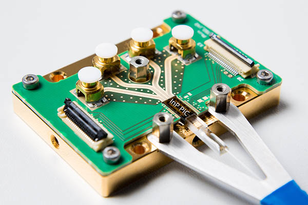
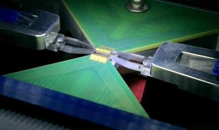
Packaging of Photonic Integrated Circuits
Photonic integrated circuits generally need to be packaged in some way to be used. Packaging is widely recognized as one of the most complex and costly challenges in the integration and commercialization of photonic technologies. Some of the main challenges associated with PIC packaging are the following:
- Optical alignment and coupling: Efficiently coupling light between PICs and optical fibers or other components requires sub-micron tolerances. Misalignment leads to significant insertion loss.
- Different coupling methods exist (e.g. edge coupling and grating coupling), which have specific limitations, e.g. in terms of spectral bandwidth, polarization sensitivity and manufacturability.
- Thermal management: As PICs integrate both active and passive components in a very dense fashion, heat dissipation and thermal crosstalk can be a major concern, especially for lasers and high-speed modulators. Thermal problems may occur concerning operational stability, wavelength drift and also component lifetime.
- High-speed electrical integration: Routing high-frequency RF signals within small packages without introducing noise, impedance mismatch or cross-talk is nontrivial. Techniques like wire bonding, flip-chip bonding and electrical interposers are used.
- Material and mechanical compatibility: Packaging materials must be compatible with photonic chips — hermetic sealing, robustness, and stability over broad temperature ranges are usually required. Mechanical stresses, especially during handling and assembly, can damage photonic structures.
- Scalability and automation: Traditional packaging processes are labor-intensive and serial, limiting throughput and scalability for large-volume manufacturing. Automated high-precision assembly solutions are still nascent, increasing production costs.
- Testing and reliability: Integrated testing during and after packaging is crucial to ensure yield and reliability under varying environmental conditions. Optical and electrical access can be restricted by packaging constraints.
- Standardization and design rules: So far, there is a lack of industry-wide standards in PIC packaging, making interoperability and mass production more difficult. Packaging design rules must be considered early in device design to avoid expensive rework and ensure compatibility with available processes.
- Hybrid and heterogeneous integration: Integrating disparate photonic materials (e.g., combining silicon photonics with III-V lasers) in the same package presents additional challenges in alignment, bonding and thermal handling.
Application Areas
Photonic integrated circuits can find applications in different areas; some examples:
- Optical fiber communications and free-space optical communications can utilize circuits for signal generation, detection, regeneration and other processing.
- Optical metrology e.g. in the form of LIDAR and fiber-optic sensors can profit from integrated circuits where even delicate devices such as interferometers can be realized in a compact and stable manner. Optical frequency metrology can utilize highly compact frequency comb sources as optical frequency synthesizers [10].
- Terahertz imaging usually involves photonic elements for generating and detecting terahertz waves and processing the signals.
- Quantum photonics is another important field of application, namely quantum cryptography and quantum computing. In some cases, photonic circuits perform only “conventional” functions like signal routing and modulation, while quantum chips perform quantum-specific functions like single-photon generation or quantum entanglement.
Very often, photonic integrated circuits are specially designed and fabricated for a specific application. They may then be called ASPIC = application-specific photonic integrated circuits.
Fabrication in Foundries
In microelectronics, the model of foundries has been widely accepted. This means a separation between a company designing and later selling an integrated circuit for a specific purpose and another company (the foundry) for fabricating it. Only the foundry needs to have the complex machinery and detailed know-how for fabrication.
The same model is also suitable for photonic integrated circuits. Again, a complex technology is required, which is mastered by some foundries, and their customers can focus on designing circuits for specific purposes and bringing those to market. A suitable interface needs to be developed, where the foundry exactly describes its capabilities and receives the designs to be fabricated. For the designs, certain elements (e.g. for realizing certain device functions like waveguides, couplers, resonators, modulators, photodetectors etc.) may already be predefined and can be appropriately connected by the circuits designer. The foundry may fabricate bare chips or possibly also offer packaging solutions.
A foundry may support different technology platforms, such as indium phosphide (InP), gallium arsenide (GaAs), silicon on insulator (SOI), silica on silicon, etc. Note that these can substantially differ in technical details of the required machinery. It can also be important to offer the combination with other technologies such as micro-electronics and micro-electromechanical systems (MEMS).
Frequently Asked Questions
This FAQ section was generated with AI based on the article content and has been reviewed by the article’s author (RP).
What is a photonic integrated circuit (PIC)?
A photonic integrated circuit (PIC) is a chip-scale device where multiple optical and often electronic components are integrated on a single substrate, analogous to an electronic integrated circuit. It is designed to manipulate and process light signals in a compact format.
What are the main materials used for making PICs?
The most common substrate materials for PICs include silicon (for silicon photonics), indium phosphide (InP), silicon nitride (Si3N4), fused silica (SiO₂), and lithium niobate (LiNbO₃), each offering distinct advantages for different applications.
Why is silicon a popular material for photonics?
Silicon is popular due to its strong refractive index contrast, which allows for dense component integration, and its compatibility with mature CMOS fabrication processes, enabling the co-integration of photonics and electronics on the same chip.
What is the main advantage of indium phosphide (InP) for PICs?
As a direct-bandgap semiconductor, indium phosphide's main advantage is its ability to monolithically integrate active components like lasers, amplifiers, and photodetectors on the same chip, creating a complete 'all-in-one' optical system.
What are quantum photonic integrated circuits (QPICs)?
Quantum photonic integrated circuits (QPICs) are specialized PICs designed for quantum photonics. They integrate components for generating, manipulating, and detecting single photons, which are essential for applications like quantum computing and quantum cryptography.
What are the biggest challenges in PIC packaging?
Major challenges in PIC packaging include achieving precise optical alignment to fibers with sub-micron tolerance, managing heat dissipation from active components, integrating high-speed electrical signals, and developing scalable, automated manufacturing processes to reduce costs.
What is the foundry model for PICs?
The foundry model for PICs separates the design of a circuit from its fabrication. A company can design a custom PIC for a specific application and have it manufactured by a specialized foundry that possesses the complex equipment and expertise for fabrication.
Suppliers
Sponsored content: The RP Photonics Buyer's Guide contains 18 suppliers for photonic integrated circuits. Among them:

⚙ hardware
PHIX has developed several packaging solutions that allow for convenient, quick and affordable prototyping of your first photonic integrated circuits (PICs). They provide a housing with electrical connections, optical interfaces, and thermal management. Hybrid assembly of auxiliary chips is also supported. Each of our standard housings have characteristics that favor certain chip dimensions and system configurations. However, if you have special requirements, we are happy to design a customized prototype package for you.

⚙ hardware
Teem Photonics offers Photonics Integrated Circuit (PIC) solutions based on its reliable, versatile and cost effective ioNext platform. Time from design-end to chip delivery is an industry best with as short as 4 weeks turn-around time.
The specific ion-exchange process enables waveguide confinement to be varied on chip. These lead to innovative WAFT series solutions for interfacing fiber arrays with silicon photonics. The ioNext technology also allows functions such as splitters, couplers, taps, mux/demux, polarizers and custom devices which can be pigtailed to SM or PM fibers.
Bibliography
| [1] | K. Minoshima et al., “Photonic device fabrication in glass by use of nonlinear materials processing with a femtosecond laser oscillator”, Opt. Lett. 26 (19), 1516 (2001); doi:10.1364/OL.26.001516 |
|---|---|
| [2] | C. Florea and K. A. Winick, “Fabrication and characterization of photonic devices directly written in glass using femtosecond laser pulses”, J. Lightwave Technol. 21 (1), 246 (2003); doi:10.1109/JLT.2003.808678 |
| [3] | S. Nolte et al., “Femtosecond waveguide writing: A new avenue to three-dimensional integrated optics”, Appl. Phys. A 77, 109 (2003); doi:10.1007/s00339-003-2088-6 |
| [4] | A. M. Kowalevicz et al., “Three-dimensional photonic devices fabricated in glass by use of a femtosecond laser oscillator”, Opt. Lett. 30 (9), 1060 (2005); doi:10.1364/OL.30.001060 |
| [5] | A. Politi et al., “Silica-on-silicon waveguide quantum circuits”, Science 320, 646 (2008); doi:10.1126/science.1155441 |
| [6] | F. A. Kish et al., “Current status of large-scale InP photonic integrated circuits”, IEEE Sel. Top. Quantum Electron. 17 (6), 1470 (2011); doi:10.1109/JSTQE.2011.2114873 |
| [7] | W. S. Zaoui et al., “Bridging the gap between optical fibers and silicon photonic integrated circuits”, Opt. Express 22 (2), 1277 (2014); doi:10.1364/OE.22.001277 |
| [8] | L. Li, “Integrated flexible chalcogenide glass photonic devices”, Nature Photon. 8, 643 (2014); doi:10.1038/nphoton.2014.138 |
| [9] | S. Bogdanov, M. Y. Shalaginov, A. Boltasseva and V. M. Shalaev, “Material Platforms for integrated quantum photonics”, Opt. Mater. Express 7, 111 (2017); doi:10.1364/OME.7.000111 |
| [10] | D. T. Spencer et al., “An optical-frequency synthesizer using integrated photonics”, Nature 557, 81 (2018); doi:10.1038/s41586-018-0065-7 |
| [11] | J. Wang et al., “Multidimensional quantum entanglement with large-scale integrated optics”, Science 360, 285 (2018); doi:10.1126/science.aar70 |
| [12] | D. Pérez et al., “Principles, fundamentals, and applications of programmable integrated photonics”, Advances in Optics and Photonics 12 (3), 709 (2020); doi:10.1364/AOP.387155 |
| [13] | X. Hu et al., “Si3N4 photonic integration platform at 1 µm for optical interconnects”, Opt. Express 28 (9), 13019 (2020); doi:10.1364/OE.386494 |
| [14] | D. J. Blumenthal, “Photonic integration for UV to IR applications”, APL Photon. 5, 020903 (2020); doi:10.1063/1.5131683 |
| [15] | J. Wang, F. Sciarrino, A. Laing and M. G. Thompson, “Integrated photonic quantum technologies”, Nat. Photonics 14, 273 (2020); doi:10.1038/s41566-019-0532-1 |
| [16] | A. W. Elshaari et al., “Hybrid integrated quantum photonic circuits”, Nat. Photonics 14, 285 (2020); doi:10.1038/s41566-020-0609-x |
| [17] | N. H. Wan et al., “Large-scale integration of artificial atoms in hybrid photonic circuits”, Nature 583, 226 (2020); doi:10.1038/s41586-020-2441-3 |
| [18] | D. Zhu et al., “Integrated photonics on thin-film lithium niobate” (review paper), Advances in Optics and Photonics 13 (2), 242 (2021); doi:10.1364/AOP.411024 |
| [19] | J. Milvich et al., “Integrated phase-sensitive photonic sensors: a system design tutorial”, Adv. in Optics and Photonics 13 (3), 584 (2021); doi:10.1364/AOP.413399 |
| [20] | C. Op de Beeck et al., “III/V-on-lithium niobate amplifiers and lasers”, Optica 8 (10), 1288 (2021); doi:10.1364/OPTICA.438620 |
| [21] | Y. Wang et al., “Photonic-circuit-integrated titanium:sapphire laser”, Nature Photonics 17, 338 (2023); doi:10.1038/s41566-022-01144-2 |
| [22] | H. Mahmudlu et al., “Fully on-chip photonic turnkey quantum source for entangled qubit/qudit state generation”, Nature Photonics 17, 518 (2023); doi:10.1038/s41566-023-01193-1 |
| [23] | Di Zhu et al., “Integrated photonics on thin-film lithium niobate”, Advances in Optics and Photonics 13 (2), 242 (2021); doi:10.1364/AOP.411024 |
| [24] | Y. Liu et al., “A photonic integrated circuit–based erbium-doped amplifier”, Science 376 (6599), 1309 (2022); doi:10.1126/science.abo2631 |
| [25] | J. Wang et al., “Toward photonic–electronic convergence based on heterogeneous platform of merging lithium niobate into silicon”, J. Opt. Soc. Am. B 40 (6), 1573 (2023); doi:10.1364/JOSAB.484460 |
| [26] | Xu Han et al., “Integrated photonics on the dielectrically loaded lithium niobate on insulator platform”, J. Opt. Soc. Am. B 40 (5), D26 (2023); doi:10.1364/JOSAB.482507 |
| [27] | X. Lu et al., “Emerging integrated laser technologies in the visible and short near-infrared regimes”, Nature Photonics 18, 1010 (2024); doi:10.1038/s41566-024-01529-5 |
| [28] | L. A. Coldren and S. W. Corzine, Diode Lasers and Photonic Integrated Circuits, John Wiley & Sons, New York (1995) |
(Suggest additional literature!)
Questions and Comments from Users
Here you can submit questions and comments. As far as they get accepted by the author, they will appear above this paragraph together with the author’s answer. The author will decide on acceptance based on certain criteria. Essentially, the issue must be of sufficiently broad interest.
Please do not enter personal data here. (See also our privacy declaration.) If you wish to receive personal feedback or consultancy from the author, please contact him, e.g. via e-mail.
By submitting the information, you give your consent to the potential publication of your inputs on our website according to our rules. (If you later retract your consent, we will delete those inputs.) As your inputs are first reviewed by the author, they may be published with some delay.