Transistor (original) (raw)
Last Updated : 23 Jul, 2025
A Transistor is one of the types of semiconductor devices that is used to conduct and insulate electric current or voltages. A transistor acts as a switch and as an amplifier.
Transistors are considered one of the key components in most of the electronic components that we use today. It is also considered one of the best inventions in the history of science and engineering. It is used to conduct electric current and voltage and also to insulate it. In this article, we will be talking about the Transistor, its types, working, Advantages and Disadvantages of a Transistor, and more.
Table of Content
- What is a Transistor?
- Types of Transistors
- Construction of Transistor
- How do Transistors Work?
- Operation of NPN Transistor
- Characteristics of Transistor
- Transistor Biasing
- Transistor Operating Conditions
- Importance of Transistors
- Advantages of Transistor
- Disadvantages of Transistor
- Applications of Transistor
What is a Transistor?
A transistor is asemiconductor that controls voltage or current flow in electronic signals and it amplifies and acts as a switch for them. Transistor consists of three layers each of which can carry a current. If the transistor is working as an amplifier then it transforms a small input current into a big output current.
- In the case of a switch****,** it can be one of any two states that are **ON or OFF to control the flow of electronic signals through an electronic device.
- A transistor is of three layers or we can say three terminals and each of them carries the current.
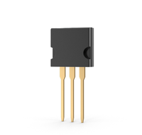
Transistor
Parts of a Transistor
As said earlier, **transistor consists of **three layers of semiconductor materials or terminals which helps to make a connection to any external circuit and all the layers do carry the current. Here voltage or current applied at any one pair of the terminals controls the current or voltage through the other pair of terminals.
There are three terminals for transistor as mentioned below:
- **Base: To activate the transistor
- **Collector: Positive lead of transistor
- **Emitter: Negative lead of transistor
Basically transistors work on the flow of current in the device from a channel to other channel.
Parts of Transistor
Types of Transistors
A Transistor can be classified into various categories, however other types of transistors are there but we are going to discuss two main types as mentioned below:
- **Bipolar Junction Transistor
- **Field effect transistor
**Bipolar Junction Transistor (BJT)
This type of Transistor is considered one of the most common types of transistors. BJT transistor consists of three terminals that is **emitter, base, and collector. It can able to amplify the electrical signal by joining all three layers into one. In current flow, there are two types of electrical charges involved i.e., electrons and holes.
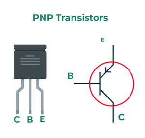
The BJT can be further classified as PNP and NPN Transistor
- **P-N-P Transistor: In P-N-P configuration the Holes are the majority charge carrier. When emitter injects holes into the transistor when the emitter-base junction is forward biased. These flow into base region which controls the current passing from emitter to the collector. The base control this flow and the collector collects the holes. By reverse biasing the collector base junction the flow is controlled which enables modulation of the collector current by the base current.
- **N-P-N Transistor: In N-P-N configuration electrons are the majority charge carriers. Electrons flow from emitter to collector when the emitter-base junction is forward biased. The base controls this flow and the collector collects the electrons. By reverse biasing the collector-base junction the flow is controlled by regulating the collector current.

BJT Symbol
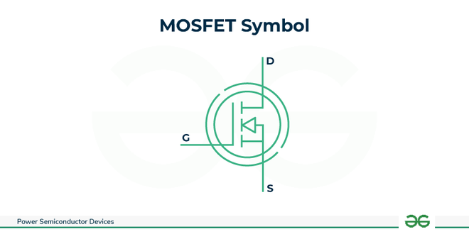
**Field Effect Transistor (FET)
This type of transistor is a **three-terminal semiconductor device. Its operation is based on a controlled input voltage. It uses an electric field to control the field of electric current in a semiconductor. They are also known as **unipolar transistors since they **contain single-carrier-type operations. FET uses either electrons or holes as charge carriers for the operation but does not use both electrons and holes. They display high input impedance at low frequencies.
There are **two types of FET as mentioned below:
- **JFET - Junction-gate FET
- **MOSFET - Metal-oxide semiconductor FET
Other Types
The BJT and FET are the main types of transistor based on how the circuit can be used, other than these two there are more types of transistor such as
- **MOSFET (Metal-Oxide-Semiconductor Field-Effect Transistor): It uses an insulated gate to control the flow of electrons.
- **JFET (Junction Field-Effect Transistor): Controls current with electric field applied across a semiconductor material.
- **IGBT (Insulated-Gate Bipolar Transistor): Combines features of both MOSFET and bipolar junction transistor (BJT) which is used in high-power applications.
- **Thin-Film Transistor (TFT): It is used in flat-panel displays and sensors.
- **HEMT (High Electron Mobility Transistor):It is used for high-speed operation and low noise performance.
- **ITFET (Inverted-T Field-Effect Transistor):It uses inverted-T-shaped gate structure for improved performance.
- **FREDFET (Fast-Reverse Epitaxial Diode Field-Effect Transistor): It is used for high-speed switching applications with low reverse recovery time.
- **Schottky Transistor: It uses Schottky barrier at the base-collector junction to improve switching speed.
- **Tunnel Field-Effect Transistor (TFET):It is used for low-power operation.
- **OFET (Organic Field-Effect Transistor):It is used for flexible electronics and displays.
- **Diffusion Transistor: It uses diffused semiconductor junction for amplification.
Construction of Transistor
A transistor is an three layer semiconductor device which is sandwiched between two same types of semiconductor. The process of sandwiching is called **fabrication of transistor.
Depending on the way of construction it is of two types as mentioned below: **PNP and NPN
**1. Construction of PNP Transistor
In this type of transistor N types transistor is sandwiched between two P types semiconductor layer as shown in the diagram. In PNP-type transistors, conduction happens through holes that carry a positive charge in other words it can conduct in the absence of electrons.
Note that current carrying collector part is less than the emitter part and base part is the one which will control the control flow between two other parts.

PNP Transistor
**2. Construction of NPN Transistor
In this particular type of transistor, P type transistor is sandwiched between two N types semiconductor layers. In **NPN-type transistors, conduction happens through electrons and not by holes. Note that electrons having a negative charge pass from the emitter to the base and are collected by the collector.
Also, the base controls the number of electrons from the emitter.

NPN Transistor
How do Transistors Work?
As we know BJT consists of three layers or terminals which are **Emitter, Base, and Collector. It is a device where two P-N junctions are there within a BJT.
- One **P-N junction exists between the emitter and base region, and the second junction exists between the **collector and base region.
- Transistors are combined to form a logic gate in which it compares multiple input current and provide output.
Transistors are used in complex switching circuits which comprise all modern telecommunication systems.
In the operation of BJT, the base-emitter is forward-biased and the base-collector is reversed-biased.
Operation of NPN Transistor
The NPN transistor is made up of n-type materials hence the majority of charge carriers are electrons that carry negative charges. When the base-emitter is forward biased then the electrons will move from the n-type region to the p-type region and the minority charge carriers (holes) will move to the p-type region. If they combine and meet together they enable a current to flow across the junction. If the junction here is reverse biased then charge carriers move away from the junction. In this case depletion region will form between two areas and there will be no current.

NPN Transistor
If the current flows between the base and emitter then the electrons will move from the emitter to the base region. Note that electrons will combine if they reach the upper region. If the electrons travel without recombining with holes then electrons will drift towards the collector. In this way charge carriers respond and react and current flows in the collector circuit.
Also read: PNP transistor for further detail.
Characteristics of Transistor
It represents the plot or structure which represents the relation between current and voltage of a transistor in a specific configuration. The characteristics of a Transistor are:
- **Input Characteristics: It gives the information about the change in input current with varying voltage having constant output voltage.
- **Output Characteristics: It is a plot of an output current with output voltage having constant input voltage.
- **Current Transfer Characteristics: This graph shows the relation between output current and input current by keeping the voltage constant.
1. Input Characteristics
**CB Configuration: The diagram given below will describe the variation of emitter current with base emitter voltage, by keeping collector voltage as constant.
CB Configuration
**CC Configuration: The graph given below shows the variation in current in accordance with voltage by keeping collector emitter voltage as constant.
CE Configuration
**CE configuration: It shows the variation in current in accordance with voltage by keeping collector emitter (Vce) voltage as constant.

CE Configuration
2. Output Characteristic
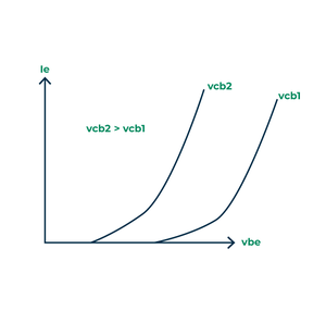
**CB configuration: The graph given below exhibits the variation in emitter current (Ie) against the changes in Vce by keeping Ib constant.

CB Configuration
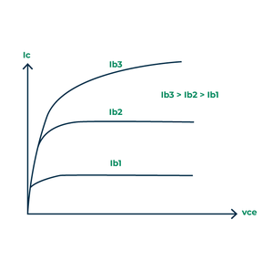
**CC configuration: In this graph it shows the variation in Ic with changes in Vce by keeping Ib as constant.

CC Configuration
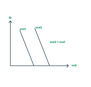
**CE configuration: The graph shows variation of Ic with the Ie by keeping Vcb as constant.
CE Configuration
3. Current Transfer Characteristics
**CB Configuration: This graph shows the variation of collector current IC with VCB ,when IE is constant.
.webp)
CB Configuration
**CC Configuration: This graph shows the variation of IE with IB , when VCE is constant.
.webp)
CC Configuration
**CE Configuration: This graph shows the variation of IC with IB ,when VCE is constant.
.webp)
CE Configuration
Transistor Biasing
It is a process of applying a DC operating voltage condition to the transistor so that the AC input signal can be amplified correctly by the transistor. It is one of the most used semiconductor devices that is used for a wide range of applications. To obtain those functionality a transistor must be supplied with current or voltage. It can be accomplished by various biasing circuits and techniques.
Types of Transistor Biasing
Well, in this particular context we will see types of transistor biasing and the most common preferred methods for biasing of transistor are as mentioned below.
- **Base Resistor: The base terminal of the transistor is connected with a high value of the base resistor and the transistor used in the circuit is of NPN type so that the other end of the resistor will be connected to the positive part of the supply. It makes the junction base-emitter to be forward biased and the terminal base will be positive compared to the emitter terminal.
- **Collector To Base: In this collector-to-base biasing the circuit consists of a base resistor which is fed back to the terminal collector. It is different from the method of base resistor. Note that if the current at the collector tends to increase the voltage at the load resistor gets increased which results in an increase in the value of the voltage at the collector-emitter and the current at the base will be reduced.
- **Voltage Divider: This type of biasing is widely preferred because it consists of two resistors. This biasing helps in providing stabilization due to the resistor present at the emitter and one disadvantage of using this type of biasing is here the signals tend to get mixed while using this bias in the circuits.
Transistor Operating Conditions
When a small signal is applied between one pair of terminals in a transistor, a signal can be operated to control a much larger signal at another pair of terminals. In this part, the property of the transistor is gained due to signal strength in the process of switching and the output generated can be either voltage or current or electronic signal. If the input increases then the output also increases. In other words, it is simple to say that output is proportional to input. Due to this particular activity transistor can act as an amplifier.
The main use of a transistor is that it makes the circuit more controllable and the current flow is determined by other circuit elements. Depending on the biasing conditions like forward or reverse, transistors have three major modes of operations cutoff, active, and saturation regions.
- **Active Mode: In this mode, the transistor is generally used as current amplifier. In active mode, two junctions are differently biased which means **emitter-base junction is forward biased whereas collector-base junction is reverse biased. In this mode, current flows between emitter and collector and the amount of current flow in proportional to the base current.
- **Cutoff Mode: Here **both collector base junction and emitter junction are reverse biased. As both the PN junction are reverse biased, there is almost no current flow except very small leakage of currents. In BJT mode it is switched OFF and is essentially an open circuit. This region is mainly used in switching and digital logic circuits
- **Saturation Mode: In this particular mode of operation, **both the emitter-base and collector-base junctions are forward biased. Here current flows freely from collector to emitter with almost 0 resistance. In this mode, the transistor is fully switched ON and it is a closed circuit. It is mainly used in switching and digital logic circuits.
.png)
BJT Region of Operation
Importance of Transistors
- As we are aware, transistors are used for building simple electronic switches. They are considered as basic elements in integrated circuits. To build a microprocessor, various numbers of transistors were embedded into a single Integrated circuit.
- Transistor is mainly used for high-power applications and low frequency such as power supply adapters. In modern telecommunication systems, transistors act as **complex switching circuits.
- Transistors are semiconductor devices that are used for modern electronic equipment to switch signals. It is considered a building block of modern electronic machinery which is manufactured from semiconductors.
- As we know transistors consist of three terminals which are used to control the voltage and current at the two terminals. Today more transistors are found in embedded C.
Advantages of Transistor
Here are some advantages of a transistor:
- It has a low operating voltage and extremely long life.
- It does fast switching and has no power consumption.
- By using transistors, better efficiency of circuits can be developed.
- It is used to develop integrated circuits.
- It is smaller in size and lower in cost.
Disadvantages of Transistor
Here are some disadvantages of a transistor:
- If the switching frequency is high then the transistor has greater loss of power.
- It generates high amount of heat and breaks down the circuit.
- It is sensitive to radiations (cosmic rays).
- It is difficult to identify the type of error and repair faulty transistors due to small in size.
- Transistors produce little energy which is not sufficient for electronic signals and devices.
Applications of Transistor
Transistors are fundamental building blocks of modern electronics. They are essentially tiny, solid-state switches that can amplify or regulate a current or voltage. Here are some of their key applications:
- **Switch: Transistors can function like electronic switches. By applying a small voltage, a large current flow can be controlled on or off. This capability is crucial for digital circuits, the foundation of modern computers and many other devices.
- **Amplifier: Transistors can take a weak electrical signal and make it much stronger. This is essential for applications such as hearing aids, amplifiers for musical instruments, and radio technology.
- **Integrated Circuits (ICs): Transistors are miniaturized and embedded in large numbers onto tiny silicon chips to create complex integrated circuits. These ICs are the heart of modern electronics, found in everything from smartphones and computers to cars and medical devices.
- **Memory: Transistors are used in various memory devices, such as Random Access Memory (RAM) and Flash memory, which enable electronic devices to store and retrieve data.
- **Logic Gates: Transistors can be combined to form logic gates, the basic building blocks of digital circuits. Logic gates perform basic operations like AND, OR, and NOT, which allows for complex computations within electronic devices.
Conclusion
In this particular article we have seen in detail about the transistor, its types, working principle and its application. Transistors play a vital role in this digitalized world as it helps to improve the efficiency of operational electronic signals and make more compact electronic devices and so on.
So a transistor is used as a switch in the circuit , as the base voltage goes high then current flow from collector to emitter and then transistor gets switch on and as the current stops flowing then the transistor gets off.