NPN Transistor (original) (raw)
Last Updated : 23 Jul, 2025
An NPN Transistor is a Negative-Positive-Negative transistor that has a significant and varied impact on electronic circuits. The NPN transistor is made up of three semiconductor layers that are arranged in a particular way. One of the layers is of the positive (P) type and is sandwiched between two of the negative (N) types. Electrons flow from the N-type region through the P-type region when a voltage is applied across the transistor's terminals, resulting in controlled conductivity and allowing the transistor to act as an amplifier or switch. Hence, its name is derived from this distinctive arrangement.
- The transistor can control the flow of electric current because of its layered structure, which serves as the foundation for its operation.
- A bipolar junction transistor (BJT), a crucial semiconductor component of electronic circuits, is a type of transistor with NPN configuration.
- In contrast, the collector-base junction is biased in the opposite direction. This indicates that the electron flow is inhibited by the voltage applied here.
However, the electric field removes the majority of electrons that successfully cross the emitter-base junction across the collector-base junction, amplifying the current flowing from the emitter to the collector.
Symbol of NPN
The Symbol for NPN can be given as
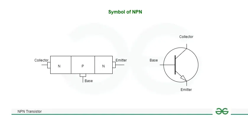
Symbol of NPN
Bipolar NPN Transistor Configuration
The NPN transistor is supported by three layers, two of which are P-type transistors and the other two of which are N-type transistors. While it's often simplistically described as semiconductors are formed by connecting two diodes sequentially, this analogy is primarily for conceptual understanding rather than an exact representation of the transistor's structure.
- As each diode has two doped areas, the subsequent structure will have four doped locations if it is formed by connecting two diodes one after the other.
- Since uniform doping is a prerequisite for the transistor the base formed by associating it consecutively will not have this condition.
.png)
Common Emitter Configuration
- As a result, there are always three layers: the first is lightly doped, like base, the second is heavily doped, like Collector, and the third is Emitter, which is decently doped.
- The Collector and Emitter of the P-type are sandwiched between the foundation of the N-type. As a result, a transistor of the N-type is created.
- The emitter, base, and collector are the three layers that make up an NPN transistor.
- For the transistor to function properly, each layer plays a distinct role. The N-type layer is the emitter and the electron source. The electron flow from the emitter to the collector is controlled by the base, which is typically a thin P-type layer.
- The electrons are collected by the collector, another P-type layer, which completes the circuit.
- The movement of charge carriers, particularly electrons, across the NPN transistor's layers is fundamental to its operation.
- Whenever a voltage is applied across the producer base intersection (forward-one-sided), it permits electrons to move from the N-type producer to the P-type base.
- To make electron transit more likely, the base region is intentionally thin.
Working of NPN Transistor
- Forward bias should be used at the base-emitter junction, and reverse bias should be used at the collector base intersection. As a result, the negative terminal of the VBE is linked to the N-terminal of the emitter-base intersection, and the positive terminal of the battery is linked to the P-terminal of the VBE.
- The N-terminal is connected to the VCB's positive terminal to invert the authority base intersection, while the P-terminal is connected to the battery VCE's negative terminal. As a result, the gatherer base intersection will have a wide exhaustion layer and the emitter base intersection will have a limited consumption layer.
- The electrons in the N-area will repel from the battery's negative terminal and move toward the base region when forward bias is applied to the emitter-base junction. When compared to the area of the emitter and collector, the base area is very small. Additionally, the base's doping force is greatly diminished. As a result, there are fewer holes in it.
- A few electrons and holes will recombine due to the absence of many holes in the base region. Various electrons that have not yet recombined will move toward the gatherer district.
- This will include the circuit's current. Because of its enormous size, the gatherer can dissipate heat and gather additional charge transporters. Since electrons are the primary charge transporters in the NPN transistor, the current is caused by electrons. The emitter current in an NPN semiconductor is equivalent to the amount of base and gatherer current. Numerically it tends to be composed as:
IE = IB + IC
- In NPN transistor , in the common emitter configuration, the emitter is doped heavily compared to that of collector and current flows from base to emitter , as NPN transistor is used in CE configuration as an amplifier so we will discuss it in detail:
Common Emitter Configuration
- The base is the input terminal in a common emitter configuration, the collector is the output terminal, and the emitter is the common input and output terminal. This indicates that the collector terminal and the common emitter terminal are referred to as output terminals, while the base terminal and the common emitter terminal are referred to as input terminals.
- In like manner producer design, the producer terminal is grounded so the normal producer setup is otherwise called grounded producer arrangement.
- Common emitter configuration, common emitter amplifier, and CE amplifier are also sometimes used interchangeably. The most common transistor configuration is the common emitter (CE) configuration.
- When a significant current gain is required, common emitter (CE) amplifiers are utilized.
- The base and emitter terminals receive the input signal, while the collector and emitter terminals receive the output signal. The term "common emitter configuration" refers to the fact that a transistor's emitter terminal serves as both the input and output terminal.

Common Emitter Configuration
- VBE is the supply voltage between the base and the emitter, and VCE is the supply voltage between the collector and the emitter.
- IB stands for input current, also known as base current, and IC stands for output current, also known as collector current, in a configuration known as common emitter (CE).
- The input and output impedance levels of the common emitter amplifier are moderate.
Therefore, the common emitter amplifier has a voltage gain and current gain that are medium. However, the gain in power is substantial. We require two sets of characteristics—input characteristics and output characteristics—to fully describe the behavior of a transistor with CE configuration.
α and β Relationship in a NPN Transistor
DC Current Gain = Output Current/Input Current = IC/IB
using KCL
IE = IB + IC
α = IC/IE
so,
β can be calculate as
β = IC/IB = IC/IE(1-α) = α/(1-α)
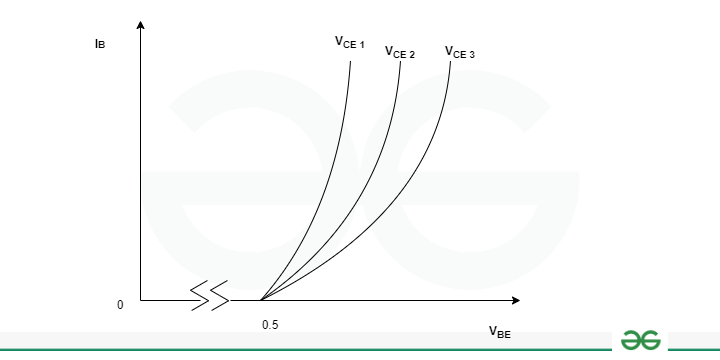
**Input Characteristics of NPN Transistor: Input characteristics refer to the curve between base current and base-emitter voltage for a particular collector-emitter voltage value.
**Output Characteristics of NPN Transistor: In below figure shows the output characteristics of an NPN transistor. The curves show the connection between the collector current (IC) and the collector-emitter voltage (VCE) with the differing base current (IB). We realize that the semiconductor is 'ON' just when essentially a modest quantity of current and a limited quantity of voltage is applied at its base terminal compared with a producer in any case the semiconductor is in an 'OFF' state.

Output Characteristics of NPN Transistor
The collector current (IC) is for the most part impacted by the collector voltage (VCE) at 1.0V level however this IC value isn't exceptionally impacted over this value. As of now, we realize that the emitter current is the amount of base and collector current. for example IE =IC+ IB. The ongoing coursing through the resistive load (RL) is equivalent to the authority current of the semiconductor. The condition for the authority current is given by,
IC= (VCC-VCE)/RL
The straight line demonstrates the Dynamic load line which is interfacing the focuses A (where VCE = 0) and B (where IC = 0). The region along this heap line addresses the 'active area' of the transistor. The common emitter design attributes bends are utilized to ascertain the gatherer current when the collector voltage and base current are given. The heap line is utilized to decide the Q-point in the diagram. The incline of the heap line is equivalent to the proportional of the heap opposition. i.e. -1/RL.
Applications of NPN Transistor
- **Voltage Regulation: In specific arrangements, NPN transistors can be utilized for voltage guidelines, adding to stable power supply yields.
- **Current Regulation: NPN transistors can be utilized to manage or control the progression of current in a circuit, tracking down applications in current sources and consistent current circuits.
- **Amplification: NPN transistors are usually utilized for signal enhancement in electronic circuits. They are essential parts of sound enhancers, where powerless info signals should be helped for driving speakers.
- **Amplitude Modulation: NPN transistors assume a part in plentiful changes (AM) circuits, a procedure utilized in simple correspondence.
- **Switching: NPN transistors act as electronic switches in advanced circuits. By controlling the base current, a huge current can be permitted to stream between the gatherer and producer.
- **Oscillation: NPN transistors are used in the development of oscillators, which create ceaseless waveforms. This application is fundamental in electronic gadgets like radio-recurrence (RF) oscillators.
Advantages of NPN Transistors
- **Compact In Size: NPN transistors are generally small in size, adding to the scaling down of electronic gadgets and coordinated circuits.
- **Amplification: NPN transistors give proficient sign enhancement, making them reasonable for a large number of sound and electronic applications.
- **Speed Switching: They offer quick exchanging speeds, making them ideal for advanced applications where fast changes among on and off states are important.
- **Cost-Effective: NPN transistors are cheap to use in electronic gadgets.
- **Versatility: Their adaptability considers different arrangements, making them versatile to various circuit plans and applications.
Disadvantages of NPN Transistors
- **Reversal of Sign: The resulting signal is many times reversed concerning the info signal, which might require extra hardware for signal remedy in certain applications.
- **Heat Generation: NPN semiconductors can produce heat during activity, and in high-power applications, extra-intensity scattering systems might be required.
- **Temperature Sensitivity: The qualities of NPN semiconductors are delicate to temperature varieties, which can affect their exhibition.
- **Complexity in Design: High-level applications might require complex circuit plans and biasing courses of action, which can be trying for fledglings.
- **Power Limits: In high-power applications, different advances like MOSFETs might be liked over NPN semiconductors because of their lower power taking care of capacities.