Capture Asynchronous Data - MATLAB & Simulink (original) (raw)
Main Content
Use FPGA data capture to observe signals operating at different clock rates from your design while the design is running on the FPGA. The FPGA data capture feature captures the asynchronous data by using multiple FPGA data capture IPs.
Note
You can enable multiple data capture IPs only when targeting the AMD® devices over a JTAG interface.

Use the FPGA Data Capture Component Generator tool to generate multiple data capture IPs. Add the generated IPs and the JTAG Debug Hub IP to the Vivado® user repository by using the addFPGADataCaptureToVivado function. Then, to capture the asynchronous data, manually integrate these IPs into your Vivado project and deploy them to the FPGA along with the rest of your design. The JTAG Debug Hub IP communicates with MATLAB® on the host machine and with each data capture IP in the FPGA design.
Configure and Generate Data Capture IPs
Use the FPGA Data Capture Component Generator tool to configure and generate the data capture IPs. In the tool:
- Set FPGA vendor to
AMDandConnection type toJTAG. - Set Number of data capture IPs to a value greater than 1.
- Specify a unique name for each data capture IP by using the Generated IP name parameter.
- Specify the port names and sizes for each data capture IP. These ports connect to the signals that you want to capture and the signals that you want to use as triggers for each capture.
- Select storage type as either internal memory or external memory. Internal memory uses internal BRAM resources to store captured data, while external memory uses external DDR memory connected to the FPGA for storage.
- Specify how many samples to return, maximum number of trigger stages, and whether to include capture condition logic for each data capture IP.
- Specify whether to include trigger input and output ports to each data capture IP. Use these ports to pass the trigger signal from one data capture IP to another.
- Click Generate.
The tool generates these data capture components in the specified destination folder:
Specific to Data Capture IP
- Packaged IP core, for integration into your FPGA design. Each IP core contains:
- A port for each signal you want to capture or use as part of a trigger condition.
- Memory to capture the number of samples you requested for each signal.
- An interface logic (BSCAN subordinate interface) to communicate with the JTAG Debug Hub IP.
- Trigger and capture condition logic that can be configured at run time.
- A ready-to-capture signal to control data flow from the FPGA.
- An FDC_active signal to control data capture IP from the JTAG Debug Hub IP.
- Generation report, with list of generated files and instructions for next steps.
- Tool to set capture parameters and capture data to the MATLAB workspace.
- Customized version of the data capture System object™ that provides an alternative, programmatic, way to configure and capture data.
- MAT file in the
_`generatedIPName`__generation_settings.matformat, where_`generatedIPName`_is the name of the generated data capture IP. This MAT file holds the data capture build parameters to reload the same design in your next iteration.
Common to All Data Capture IPs
- Tool to set capture parameters for all the data capture IPs and to capture multiple data signals to the MATLAB workspace.
- MAT file,
multipleDatacaptureIPs_gensettings.mat, which holds the build parameters for all the generated data capture IPs. To reload the same design in your next iteration, provide this MAT file as an input argument to the generateFPGADataCaptureIP function.
Add Generated IPs to Vivado Project
Add the generated packaged IP cores and JTAG Debug Hub IP to the Vivado user repository by using the addFPGADataCaptureToVivado function.
- Create a Vivado project.
- Add HDL IPs in the specified folder to the specified Vivado project.
addFPGADataCaptureToVivado("vivadoProjectPath",DataCaptureIPFolder="destinationFolder");
Where_`vivadoProjectPath`_is the name of Vivado project location and_`destinationFolder`_is the name of the folder that contains the generated IP cores.
For example, the following command adds the data capture IPs and JTAG Debug Hub IP in thehdlsrcfolder to theC:\test_design_zc706\hdl_prj\vivado_ip_prj\vivado_prj.xprVivado project.
addFPGADataCaptureToVivado("C:\test_design_zc706\hdl_prj\vivado_ip_prj\vivado_prj.xpr", ...
DataCaptureIPFolder="hdlsrc");
Integrate Generated IPs into Vivado Design
To capture FPGA data, integrate the data capture IPs into your Vivado design. The host computer communicates with the JTAG Debug Hub IP and you must connect all the data capture IPs to the hub IP. To integrate the IPs, follow the instructions in the generation report.
- Open the Vivado project.
- Add the data capture IPs and the JTAG Debug Hub IP to the Vivado block design.
- Connect the BSCAN subordinate (BSCAN_S) interface of each data capture IP to the BSCAN manager (BSCAN_M) interface of the JTAG Debug Hub IP.
To enable multiple BSCAN manager interfaces of the JTAG Debug Hub IP, in the hub IP, setNumber of DataCapture IPs to the required value. - Connect the
dc_activeoutput port of each data capture IP to the respective active (active_s) input port of the JTAG Debug Hub IP.
- Versal® only — Insert the AMD Versal platform CIPS IP into your block design. Connect the BSCAN subordinate (BSCAN_S) interface of the JTAG Debug Hub IP to the BSCAN_USER2 interface of the CIPS IP. To enable the BSCAN_USER2 interface, enable the PL BSCAN1 interface in the CIPS IP.

- Make sure that the data capture ID of each data capture IP is unique and matches with the
DataCaptureIDof corresponding data capture System object.
To update the data capture ID, in the data capture IP, set datacapture ID to the required value. - External memory only — For non-Versal devices, connect the AXI4 manager (AXI4_M) interface of each data capture IP to the AXI4 subordinate (S_AXI) interface of MIG through AXI Interconnect as this figure shows.

For Versal devices, connect the AXI4 manager (AXI4_M) interface of the data capture IP to the AXI4 subordinate (S_AXI) interface of the AMD AXI NoC IP as this figure shows.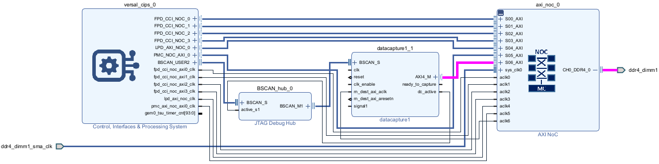
- Connect data capture IPs to the signals you requested for capture and triggers.
- Complete the block design by connecting the
clkandclk_enableinput ports of the data capture IPs. Additionally, for external memory, connect theAXI4_M_ACLK,AXI4_M_ARESETN, andIPCORE_RESETNinput ports of the data capture IP. - External memory only — Make sure that the
AXI4_M_ACLK, used by the data capture IP to write data to external DDR memory, has a higher frequency than theclkclock. - Compile the project and program the FPGA with the new image through a JTAG cable.
Capture Asynchronous Data
The JTAG Debug Hub IP communicates over the JTAG cable between your FPGA board and the host computer. Make sure that the JTAG cable is connected. Before capturing asynchronous data, in theFPGA Data Capture tool, you can set data types for the captured data, number of windows to capture, set trigger condition that specifies when to capture the data, and set a capture condition that specifies the data to be captured for each data capture IP.
- Trigger — When the design is running on the FPGA, first the JTAG Debug Hub IP waits for the trigger condition that you specify. Define a trigger condition by specific values matched on one or more signals. When the trigger is detected, the logic captures the designated signals in a buffer and returns the data over the JTAG interface to the host machine.
- Capture Condition — To make the best use of the buffer size and capture only the valid data, you can also define a capture condition. Define a capture condition in the same way as you define the trigger condition. When both the trigger is detected and the capture condition is satisfied, the logic captures only the valid values of the designated signals.
To configure these options and capture data, you can:
- Open the FPGA Data Capture tool by executing this command in MATLAB.
launchMultipleDataCaptureApp
Set the trigger, capture condition, and data type parameters for each data capture IP. Then, capture data into the MATLAB workspace. - Use the data capture System object generated for each data capture IP.
- Create a dataCaptureHub object, which can interact with each data capture System object.
- Add all the data capture System objects to the hub object by using the addDataCaptureIP function.
hub.addDataCaptureIP("dataCaptureSystemObjectPath");
Where_`dataCaptureSystemObjectPath`_is the name of the data capture System object location.
For example, the following command adds the System object of thedatacapture1data capture IP to thehubobject.
hub.addDataCaptureIP("datacapture1\datacapture1.m"); - External memory only — Set the base address of the external DDR memory for each data capture IP by using the setMemoryBaseAddress function.
For example, the following command sets the base address of the DDR memory for thedatacapture1data capture IP to80000000.
setMemoryBaseAddress(hub,"80000000",DataCaptureName="datacapture1");
Set the data types, trigger condition, and capture condition using the object functions and properties of the System object for each data capture IP, and then call the hub object to capture data.
After you capture the data and import it into the MATLAB workspace, you can analyze, verify, and display the data.