image sensors (original) (raw)
Definition: optoelectronic sensors which can be used for imaging
Alternative terms: imaging sensor, imager
Categories:  photonic devices,
  optoelectronics,
  vision, displays and imaging
- image sensors
Related: camerasphoto camerasimagingphotodiode arraysfocal plane arrays
Page views in 12 months: 1346
DOI: 10.61835/83w Cite the article: BibTex BibLaTex plain textHTML Link to this page! LinkedIn
Content quality and neutrality are maintained according to our editorial policy.
📦 For purchasing image sensors, use the RP Photonics Buyer's Guide — an expert-curated directory for finding all relevant suppliers, which also offers advanced purchasing assistance.
Contents
What are Image Sensors?
Image sensors are optoelectronic sensors that measure light intensities in a spatially resolved manner for imaging applications. They are used in various kinds of cameras and in scanners, for example
- in digital photo cameras
- in video cameras (television, consumer devices, surveillance, industry, etc.)
- for thermal imaging (thermography)
- for various kinds of scanners such as document scanners
Some image sensors generate only one-dimensional images, but by combining multiple such images with consistent transverse spacings, one can assemble two-dimensional images. For example, that is often done in document scanners. Other sensors directly produce two-dimensional images.
Image sensors are also called focal plane arrays (FPAs), indicating that they are detector areas placed in the focal plane of an imaging system.
Important Properties of Image Sensors and Their Optimization
Before explaining concrete sensor types, we consider various properties of sensors which determine their performance.
Light Sensitivity, Fill Factor and Quantum Efficiency
It is often desirable to achieve sufficient signal strength with a limited amount of light to limit the required exposure time. Therefore, one tries to obtain a high quantum efficiency of the detection.
The light-sensitive parts of CMOS or CCD chips can have a quite high quantum efficiency, often around 80% or even 90% over the visible spectral range. However, some of the light is often lost because the light-sensitive parts do not cover the full pixel area. That problem of a limited fill factor can be reduced either by minimizing the size of light-insensitive parts or by properly directing the incident light to the sensitive regions, e.g. using microlens arrays. The latter approach, however, can have detrimental side effects, such as an increased directionality of the sensitivity (the relevance of which depends on the used optical camera design) and smear effects due to optical cross-talk between different pixels. Certain wedge structures have been developed which are better in that respect.
Another approach is backside illumination through a substrate of reduced thickness. That principle has been applied successfully both to CCD and CMOS sensors.
Note that the term sensitivity is often erroneously used instead of responsivity. The sensitivity also depends on image noise, which can have different origins:
- Shot noise related to photon statistics can play a role in sensitive applications. If a detector collects a certain number of carriers within the measurement time on average, there will be an uncertainty (standard deviation) which is the square root of that number.
- Thermal noise may not only cause a dark current (for operation with some bias voltage), but also affects the charge measurement: when the capacitor is discharged at the beginning of the measurement period, it will not be perfectly discharged, but rather hold some thermal energy, which causes thermal noise in the measurement result — unless the initial voltage is measured as well and subtracted from the result (which is sometimes done).
- The charge amplifier may add some further noise, which is partially also thermal noise.
- There can be systematic deviations between different pixels due to microscopic parameter variation; such fixed pattern noise may be eliminated after each measurement with software.
For highest sensitivities, e.g. in astronomy, image sensors often have to be cooled to reduce thermal noise. With proper optimization of the whole system, photon noise limited performance can be achieved.
Sensor Formats
Image sensors are available with a wide range of formats. Sensors for miniature cameras as used in smart phones are only a few millimeters wide, while an SLR photo camera typical has a sensor with a width of the order of 30 mm. Frequently, the sensors are significantly smaller than the full format size of 36 mm × 24 mm (where the crop factor indicates the reduction in diagonal size), but there are also full-size sensors and even sensors in substantially larger sizes.
The ratio of width to height is often 4:3 or 16:9 corresponding to frequently used image formats. However, other formats like 1:1 and 2:1 are also available for special purpose cameras.
Spatial Resolution and Pixel Pitch
The resolution of an image sensor is simply specified by the number of pixels in the horizontal and vertical direction — for example, 1024 × 768 or 1600 × 1200.
The pixel spacing (pixel pitch) in CMOS or CCD sensors is typically somewhere between 2 μm and 30 μm. For example, if a consumer-type photo camera contains an image sensor with 3000 × 2000 pixels, which is 24 mm wide, the pixel spacing is 24 mm / 3000 = 8 μm. (The height and the width of the pixels should normally be identical.) The pixel size can be somewhat smaller than the pixel pitch; not the whole chip area is active area.
Obviously, the pixel spacing should be small enough to exploit the full resolution potential of the optical part, while on the other hand it does not make sense to make it significantly finer, since that would not only increase the fabrication cost but also unnecessarily increase the amount of data to be handled and possibly also reduce the fill factor and thus the efficiency. However, there are some technical approaches (e.g. quantum image sensors, see below) where a rather small pixel size can still make sense.
Dynamic Range, Linearity, Overflow Effects
The dynamic range of an image sensor (usually specified in decibels) is the range of intensities which a pixel can measure. The maximum for a CCD or CMOS sensor, for example, is set by the full-well capacity, while the minimum is often defined by readout noise.
For sensors with an integrated analog-to-digital converter (e.g. CMOS sensors), there is also quantization noise related to the number of bits. For example, a 14-bit sensor can deliver 214 = 16,384 different intensity values, corresponding to a dynamic range of 42 dB. The actual dynamic range may be smaller; the lowest bits are often meaningless, e.g. due to readout noise.
Dynamic range may not be a fixed quantity for a specific sensor, as it can depend on operation modes.
Depending on the details of the electronics, CCD or CMOS chips can be highly linear throughout the dynamic range, or exhibit substantial nonlinearities. The type and quality of the charge amplifier can be important for that aspect.
For excessive illumination beyond the full well capacity of a pixel, there can be blooming effects by overflow of carriers to neighboring pixels.
Cross-talk
Cross-talk means that light hitting one pixel also produces some response on other pixels. This may happen in the form of optical cross-talk, e.g. by scattering of light at microlenses. Also, cross-talk can occur in the electronics, particularly at high light levels.
Pixel Defects
Particularly for CMOS sensors, but also for CCD sensors it can happen that certain pixels are defect, e.g. always delivering maximum signal even with no incident light, or always zero signal. That may not always be immediately noticed, but even consumer cameras should of course not exhibit a substantial number of dead pixels. To some extent, dead pixel effects can be mitigated with electronics — for example, delivering data of neighboring pixels instead of consistently wrong values.
Readout Time and Frame Rate
The time for readout of a complete image frame can be substantial, particularly for a high-resolution CCD sensor with many millions of pixels. That limits the possible frame rate of a video camera, for example.
Therefore, the multi-tap technique has been developed for CCD sensors, where different parts of the image are transmitted in parallel through two, four or even more outputs. However, this can lead to problems because one then requires multiple charge amplifiers and A/D converters, which may somewhat deviate in performance parameters, producing image artifacts.
CMOS sensors are generally faster, and there are versions for several thousands images per second.
Compatibility with Objectives
For a photo camera, for example, it is important that the used image sensor fits well to the used photographic objective. For example, objectives are optimized for a certain image sensor format. Also, the incidence angle of light on the sensor can depend on the objective, and some sensors (e.g. with microlenses) may not work well with larger incidence angles; they should be used in conjunction with telecentric lenses.
Linear Image Sensors
Photodiode Arrays
If only a relatively small number of pixels is required, a photodiode array can be used. It contains one photodiode per pixel, and all those diodes are addressed with separate wires. Usually, one has a line sensor, with all pixels arranged in a single row.
This simple approach is no longer practical for line sensors with thousands of pixels because the number of wire connections would be excessive. Even if suitable connectors could be made, further processing of the data (e.g., with a microprocessor) would be inconvenient.
Photodiode arrays are available with different kinds of photodiodes to be used for specific spectral regions. For example, there are silicon arrays for use with visible or near-infrared radiation, whereas with indium gallium arsenide devices one gets further into the infrared.
Line Sensors with Sequential Readout
For high-pixel-count line sensors (as used in line-scan cameras), one replaces parallel readout with a serial readout so that pixel signals are transmitted sequentially in time.
It would not be most practical to realize such a technique for photocurrents — providing an output current which at some time corresponds to the photocurrent of a particular photodiode. The same holds for concepts based on electric voltages. Instead, the common method is to work with electric charges instead of currents; such charges are accumulated within a certain exposure time (which may of course be adjusted to the measurement conditions).
Electronic image sensors are fabricated as optoelectronic semiconductor chips. Each pixel contains a photodetector that charges a capacitor during exposure; the charge (or change in charge from a preset bias) reflects the collected light.
Eventually, charge is converted into a voltage. Different approaches are used for that conversion — most prominently the CMOS and CCD concepts described below. These are typically silicon-based and therefore sensitive across the visible spectrum and somewhat into the infrared.
Linear CMOS Sensors
CMOS means complementary metal–oxide–semiconductor — a technology used to make integrated circuits. The same technology underlies CMOS image sensors. The photodetector can be a photodiode or a photogate.
Early CMOS sensors used passive pixel sensors (PPS), where a single MOS transistor connects each photodetector to a shared charge amplifier. This yields simple designs with a high fill factor.
Modern active pixel sensors (APS) have a charge amplifier associated with each pixel, improving signal-to-noise ratio and speed. Additional transistors are often used for functions like global shuttering and noise suppression. Some designs even include per-pixel analog-to-digital conversion (“digital pixel sensors”) with output to a digital bus, eliminating downstream analog degradation.
Although full-frame sequential readout is common, CMOS allows random pixel/region access (e.g., reading a region of interest or skipping rows for higher frame rates).
A major advantage of the CMOS sensor technology is that it can be easily integrated with additional analog or digital circuits on a CMOS chip.
Linear CCD Sensors
CCD sensors are based on the principle of charge-coupled devices, which were originally developed for purely electronic applications, but have been found to be most useful for imaging. While the light-sensitive part can be of the same kind as in a CMOS sensor, the readout method is completely different. We first consider the simpler situation of a linear CCD sensor array and treat two-dimensional CCD sensors in a later section.
A common type of implementation involves a transfer gate, which is another array structure placed parallel to the MOS sensor pixels; it is itself made light-insensitive by some shielding and acts as an analog shift register. After exposure, one first shifts the charges of the photodetectors into the transfer gate. Thereafter, one then sequentially reads out the signals from there based on the principle of the shift register. In each step, one transfers the charge from each cell of the shift register to the neighborhood one — except for the last one, where the signal is read out with a charge amplifier (normally on a separate analog chip), producing a voltage signal. In a first step after exposure, the output will reflect the amount of light received by one of the detectors; in further shifting cycles, one subsequently obtains the signals for all the other detectors. During the shifting procedure, the photodetectors may do the exposure for the next image frame.
The time-dependent voltage signal is then converted to a digital signal in an analog-to-digital converter on the same chip. Note that one requires only a single charge amplifier and analog-to-digital converter, which not only saves chip space, but also eliminates the problem of performance deviations between different pixels and reduces the frequency of pixel defects. The photodetectors themselves, having fairly simple structures, are more easily fabricated with homogeneous properties, compared with more complex multi-transistor CMOS designs.
The shift register for the charges is easy to implement with some arrangement of electrodes. Typically, it has three cells per detector pixel. Directly after transfer of the charges into the transfer gate, only every third cell contains a charge, held in a potential well created with a corresponding electrode. The potential wells can now be shifted by changing all the electrode voltages, such that each charge flows into the neighboring cell, while avoiding any mixing of charges. There are other detailed realizations of the shift register principle, but the basic principle is always as explained above.
It is also possible to combine the functions of photodetection and shift register, but then one requires an external shutter for prohibiting further illumination during the shifting operation — except perhaps if the shifting can be done much faster than the image exposure.
Usually, CCD sensor chips are complemented with additional chips for providing the required clock signal, A/D conversion, further signal processing, etc.
The importance of CCD sensor technology is underlined by the Nobel Prize in Physics 2009, which in half was given to Willard S. Boyle and George E. Smith for their invention of the principle of charge-coupled devices.
Standard Two-dimensional CMOS and CCD Image Sensors
In this section, we discuss only standard sensors, and not specific low light sensors or sensors for special spectral regions, as treated in further sections.
Two-dimensional CMOS sensors address pixels by row and column. In active pixel sensors, the addressed pixel's analog voltage is placed onto a bus. In fully digital pixel designs, digital data are transmitted instead.
Exposure of rows is often staggered (rolling shutter), but more complex designs use a global shutter, where all pixels start/stop exposure simultaneously, and are preferred for fast motion.
CMOS
Two-dimensional CMOS image sensors allow one to randomly address each pixel via its row and column number. (The number of rows or columns is often too large for addressing them with the same number of external wire connections; one needs to use a binary address code transmitted over a few wires as the input of some row or column demultiplexer.) In active pixel sensors, an analog voltage signal of the addressed pixel is sent to the bus without significant loss of signal quality. Digital pixel sensors transmit digital data instead, eliminating any loss of signal quality.
The exposure periods for the image rows are often staggered in the case of CMOS sensors; one has a rolling or scrolling shutter. However, it is also possible to realize a global shutter, which is better for use with moving objects, although it can reduce the available exposure time, e.g. in video cameras.
CCD
Two-dimensional CCDs commonly use vertical shift registers to feed a horizontal register. Each vertical transfer provides one row to read; the hard-wired order cannot be changed. Architectures include interline transfer, frame transfer, and full-frame CCDs, differing in how charges are stored and shielded during readout.
Comparison of CMOS and CCD
Due to the substantial technological developments in the areas of both CMOS and CCD sensor chips, their relative merits have changed with time and can depend substantially on what detailed devices are chosen. For example, while CMOS sensors were originally known to be less sensitive and offering lower image quality, there are now CMOS sensors which offer quite good image quality and quite similar fill factors and sensitivity. Some general differences can nevertheless be recognized:
- CMOS sensors can be more easily integrated with additional microelectronics on the same chip, providing functionality like dark current compensation and other signal processing. For example, there are devices with a logarithmic response for covering very large dynamic ranges (sometimes >60 dB). Even single-chip digital camera sensors are possible; this allows the realization of extremely compact cameras.
- CMOS cameras are generally cheaper to fabricate, particularly because less additional electronics are required.
- CMOS technology requires only a single operation voltage (e.g. 2.5 V, 3.3 V or 5 V, while CCD chips normally require higher voltages and also significantly higher electrical power (although some lower-voltage devices have also been developed).
- CMOS chips offer substantially faster readout.
- The fixed pattern noise of CMOS sensors, resulting from deviations between the electronic parts for different pixels, still tends to be higher than for CCDs. Also, pixel defects are more frequent.
Charge Injection Devices
A variant of CCD sensors are charge injection devices (CID). They are fabricated with the same MOS technology but more complex per-pixel circuitry. They also use capacitors which are discharged through illumination. The difference to CCD sensors is essentially the read-out method: The charges for the different pixels are directly read out through a bus signal, rather than sequentially coupling them to neighboring pixels. This substantially reduces cross-talk between pixels, e.g. blooming effects at high light intensity levels. Also, this approach enables random access to the pixels, i.e., it does not enforce sequential readout. Otherwise, the performance figures are similar.
CIDs are not as widely used as CCDs, but can be a favorable option for special applications, often with specially adapted designs. For example, there are devices with rather large pixel charge capacities, optimized for detection with a wide dynamic range and possibly offering quantum-limited noise. Also, there are image sensors with improved radiation tolerance.
Color Imaging
Monochrome cameras can simply use a single photodetector per pixel. For color images, several more sophisticated techniques have been developed:
- One can use dichroic beam splitters for directing the red, green and blue components of light to three separate detector chips. Such three-CCD cameras provide color images at the full resolution and good color separation, also with optimum quantum efficiency, but at a substantial cost and with a less compact setup. That principle is used for some industrial cameras and professional video cameras, but usually not for consumer photo cameras.
- One could use three different photodetectors, equipped with different color filters, for each pixel on a single chip. The substantial increase of the number of detectors is problematic, however; because the detector size cannot be arbitrarily reduced, or the chip size increased, one may get a reduced total number of pixels of the image sensor.
- A better resolution is possible with a special pattern of color filters, e.g. in the form of the common Bayer filter (named after its inventor Bryce Bayer), containing red, blue and twice as many green parts. The actual color for each pixel is then obtained with an interpolation procedure with a demosaicing algorithm. One obtains one pixel per photodetector, but of course with some significant loss of resolution and color fidelity compared with a three-CCD device. This technique is used in most photo cameras and video cameras, also in scanners.
Low-Light Sensors
Intensified Sensors
There are image sensors which are combined with an image intensifier based on a microchannel plate detector (a kind of photomultiplier) in front of the CCD or CMOS chip. This allows the operation of such intensified sensors (e.g. ICCD = intensified CCD) under very low light level conditions. However, the quantum efficiency will normally be lower, and the image noise is increased compared with operation of an ordinary sensor at higher light levels.
SPAD Arrays for Single-photon Imaging
For imaging of extremely low light levels, one may also use single-photon avalanche diodes (SPADs), operated in Geiger mode. They can now be made even in large silicon-based CMOS detector arrays. For example, they are suitable for single-photon 3D LIDAR imaging via time-of flight measurements.
Electron-multiplying CCD (EMCCD) Sensors
EMCCDs add a multiplication register (a series of high-field stages) at the end of the CCD shift path. As charge packets traverse this register, impact ionization stochastically multiplies electrons, producing adjustable on-chip gain (often on the order of 1000×) before the readout amplifier. By boosting the signal ahead of readout, the effective read noise can be reduced to sub-electron levels, enabling detection of very faint signals and even single-photon events. The gain is continuously adjustable via the clock voltages that bias the EM register.
EMCCDs can be operated in different modes:
- In “analog” electron multiplication mode, stochastic multiplication introduces an excess noise factor (≈√2), which halves SNR compared to ideal shot-noise-limited detection at the same mean signal.
- In true single-photon operation, one uses thresholding individual events at high gain and careful tuning to suppress false counts. Here, the mentioned excess noise can be largely avoided at the cost of limited dynamic range.
EMCCDs can suffer from clock-induced charge (CIC) — spurious electrons generated during high-speed clocking — especially at high gain; modern clocking and cooling minimize CIC.
EMCCDs are attractive for ultra-low-light, high-speed imaging, e.g. in single-molecule fluorescence microscopy, adaptive-optics wavefront sensing, “lucky imaging” in astronomy, and low-light spectroscopy.
Scientific CMOS (sCMOS) Image Sensors
sCMOS refers to CMOS sensors optimized for scientific high-performance imaging. Hallmarks include very low read noise (often ≈1–2 electrons r.m.s.), high frame rates, large formats, and high quantum efficiency. Special architectures are used:
- Many sCMOS sensors use a dual-gain per-pixel/column readout: A high-gain chain preserves low-level detail while a low-gain chain preserves highlights; the two are combined for wide dynamic range.
- Some sensors are optimized for ultra-low readout noise well below 1 electron in special “ultra-quiet” scan modes.
- Split-frame or column-parallel architectures allow fast readout.
- Back-illuminated (BSI) sCMOS further improves quantum efficiency (often to >90%) without microlenses, which also reduces angular dependence.
- Most sCMOS sensors use a rolling shutter by default; many offer global shutter variants/modes for motion-critical scenes.
sCMOS technology has become common for fluorescence microscopy, high-speed cell biology (e.g. bioluminescence imaging), machine vision and astronomy when “single-photon” sensitivity is not strictly required. Recent back-illuminated sCMOS devices challenge EMCCDs for many dynamic, faint-signal astronomy tasks because they avoid electron multiplication excess noise and offer higher pixel counts and frame rates.
Event-based / Neuromorphic Image Sensors
Event-based (or Dynamic Vision Sensor, DVS) pixels asynchronously report only changes in log-intensity with precise timestamps, yielding microsecond-latency “spike streams” instead of frames. Benefits include very high temporal resolution, large dynamic range, and low data rates for sparse motion. Applications include robotics, AR/VR tracking, automotive perception, and high-speed industrial inspection.
Quanta Image Sensors (QIS)
Quanta image sensors (an active research / early-commercialization area) use a special imaging paradigm. Instead of generating a conventional image frame directly, the sensor captures many rapid bit-planes (or multi-bit planes) and forms the final image by digital summing of selected planes after capture:
- In single-bit operation, each tiny pixel reports only whether at least one photon was detected during that brief integration.
- In multi-bit operation, each pixel resolves a small integer count of photoelectrons per read.
The sub-micron pixels used for this intermediate processing are called jots. Jots combine extremely low read noise (deep sub-electron) with very high readout rates. Sensors can contain hundreds of millions to billions of sub-micron jots.
Modern QIS devices are typically backside-illuminated CMOS stacks, with the jot layer on one wafer and readout/ADC on another, joined by hybrid bonding. Optimized jot designs (e.g., pump-gate structures and minimized floating-diffusion capacitance) achieve very high conversion gain, so that a single electron shifts the sense-node voltage by hundreds of µV — large enough to threshold reliably when read noise is well below one electron.
QIS readout is massively parallel (with cluster/column-parallel analog-to-digital converters), and often uses correlated multiple/double sampling to suppress noise, enabling room-temperature sub-electron read noise on large arrays.
Because each readout can occur at very low signal levels, QIS can operate effectively even when the mean signal is well below one electron per jot per read. More bit-planes (or longer temporal summing) improve the signal-to-noise ratio (SNR) at the dim end and extend dynamic range.
A key benefit is post-capture flexibility: It can be decided after acquisition how to trade signal-to-noise ratio vs. spatial resolution vs. temporal resolution by summing across jots and/or frames (spatio-temporal binning). This also enables single-exposure high dynamic range when combined with multi-bit counting or dual-gain readout.
The approach produces very high raw data rates due to fine spatial and temporal sampling. Therefore, QIS cameras rely on fast on-chip processing and smart data reduction to deliver usable image streams.
QIS combine several important performance figures:
- extremely low noise
- very fine pixel pitches for high spatial resolution
- high frame rates
- large single-exposure dynamic range (commonly reported 90 dB or more)
Limitations of QIS are the substantial design and fabrication complexity, calibration/processing demands, and heavy data throughput. As a result, the use of QIS is so far mostly restricted to scientific high-performance imaging, with early adoption in areas such as industrial and medical imaging.
Sensors for Special Spectral Regions
Although the technology of CCD and CMOS sensor chips has been driven to a very high level within several decades, it is essentially limited to silicon technology. Therefore, they are light-sensitive only for wavelengths roughly below 1 μm. Most devices are used with visible light, some also for the near infrared or for the ultraviolet region.
For infrared imaging at longer wavelengths, one requires different technologies:
- There are modified kinds of CMOS detectors, where the photodetection is done based on indium gallium arsenide (InGaAs), while the electronic processing is done with traditional silicon-based CMOS technology. The integration of different semiconductor technologies is difficult, resulting in high cost and a performance which is much reduced e.g. in terms of spatial resolution.
- For still longer wavelengths, as needed e.g. for thermal imaging, there are sensors based on micro-bolometers, which register slight heating of tiny parts caused by absorption of radiation. Such sensors are quite limited in resolution, sensitivity and speed, and are expensive.
Frequently Asked Questions
This FAQ section was generated with AI based on the article content and has been reviewed by the article’s author (RP).
What is an image sensor?
An image sensor is an optoelectronic device that measures light intensities in a spatially resolved manner. They are the core component in devices like digital cameras and scanners for capturing images.
What is the main difference between CMOS and CCD image sensors?
CMOS sensors integrate amplification and other processing circuits at the pixel level, allowing for faster readout and lower power consumption. CCDs shift charge packets across the chip to a single output, traditionally offering lower noise and higher image uniformity.
How do image sensors capture color images?
Most color sensors use a pattern of red, green, and blue color filters (like a Bayer filter) over the pixels. The sensor then uses a demosaicing algorithm to interpolate the full color value for each pixel from the data of its neighbors.
What is the difference between a rolling shutter and a global shutter?
A rolling shutter exposes and reads out pixel rows sequentially, which can distort fast-moving objects. A global shutter exposes all pixels simultaneously, capturing a single, undistorted moment in time, which is better for imaging motion.
What do quantum efficiency and fill factor mean for an image sensor?
Quantum efficiency is the percentage of photons hitting the sensor that are converted into an electrical signal. The fill factor is the fraction of each pixel's area that is light-sensitive; a higher fill factor helps capture more light.
What are EMCCD and sCMOS sensors used for?
Both are high-performance sensors for low-light conditions. EMCCDs provide on-chip gain to detect single photons, ideal for extreme low-light. Scientific CMOS (sCMOS) sensors offer very low read noise, high frame rates, and wide dynamic range for scientific applications.
What is a back-illuminated sensor?
A back-illuminated sensor is designed so that light enters through the thinned silicon substrate, bypassing the metal wiring layers on the front. This design increases light-gathering ability, leading to higher quantum efficiency.
How do event-based image sensors work?
Event-based sensors, or Dynamic Vision Sensors, do not capture traditional frames. Instead, each pixel independently and asynchronously reports when it detects a change in brightness, making them efficient for tracking high-speed motion.
What limits image sensors to certain wavelength regions?
Most CMOS and CCD sensors are silicon-based, making them sensitive only to visible and near-infrared light (below ~1 μm). For longer infrared wavelengths, sensors made from other materials like InGaAs or micro-bolometers are required.
Suppliers
Sponsored content: The RP Photonics Buyer's Guide contains 24 suppliers for image sensors. Among them:

⚙ hardware
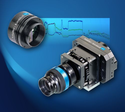
Schäfter+Kirchhoff offers line scan cameras with USB 3.0, GiGE or GiGE Vision interface. We also offer complete scanner systems like the corrosion inspector (measurement and evaluation of corrosion phenomena on coated test plates).

⚙ hardware

Hamamatsu Photonics offer 200 standard linear and area image sensors covering the short wavelength infrared (SWIR), near infrared (NIR), visible (VIS), ultraviolet (UV), and X-ray regions. With a broad selection from high speed, high sensitivity to wide dynamic range, our image sensors are suitable for different applications including spectroscopy analysis using spectrometers, industrial imaging such as machine vision cameras, microscopy, and distance measurements. We also provide supporting electronics such as easy-to-use driver circuits for sensor evaluation and driver modules for OEMs. Customizations are available for specific applications and requirements.

⚙ hardware

High-performance SPAD Technology for Next-Generation Image Sensors. We provide award-winning SPAD semiconductor technology, engineered for exceptional sensitivity and ultra-low noise. Our SPAD arrays achieve a peak photon detection probability above 50% and maintain a typical dark count rate below 100 cps. The modular design supports scalable pixel counts and customizable architectures, delivering full flexibility for tailored image sensor solutions.
Questions and Comments from Users
Here you can submit questions and comments. As far as they get accepted by the author, they will appear above this paragraph together with the author’s answer. The author will decide on acceptance based on certain criteria. Essentially, the issue must be of sufficiently broad interest.
Please do not enter personal data here. (See also our privacy declaration.) If you wish to receive personal feedback or consultancy from the author, please contact him, e.g. via e-mail.
By submitting the information, you give your consent to the potential publication of your inputs on our website according to our rules. (If you later retract your consent, we will delete those inputs.) As your inputs are first reviewed by the author, they may be published with some delay.