BJT Configurations (original) (raw)
Last Updated : 23 Jul, 2025
A transistor is also called as bipolar junction transistor or simply BJT. It is called as bipolar as only two types of charge carriers, i.e. majority charge carriers and minority charge carriers are required to perform the operations on transistor. BJT is a current-controlled device as the output voltage, current or power is controlled by the input current in the transistor. As we know, BJT is a three-terminal device , so the three configurations- we will study in this article. The three main configurations are - common emitter , common base and common collector , which has its unique characteristics and applications respectively.
Table of Content
- What is BJT?
- Configurations
- Operating regions of transistor
- Advantages
- Disadvantages
- Applications
- Comparison between CB, CE and CC configurations
What is BJT?
A bipolar junction transistor is represented by two port network. There are two types of bipolar junction transistor- NPN transistor and PNP transistor. Every transistor has three terminals- Emitter, Base and Collector.
- **Emitter: It is the outer region of the transistor. It is used to transfer charge carriers (electrons in NPN transistor and holes in PNP transistor) to the base of transistor. It is doped heavily to provide large number of charge carrier to the base.
- **Base: It is the middle region of the transistor. It is very small in length and lightly doped. Its function is to receive charge carriers from emitter and transfer it to collector region.
- **Collector: It is another outer region of the transistor. Its doping is between that of emitter and base region. It is larger than emitter region. Its function is to collect charge carriers that was provided by emitter and transferred by base.
Configurations of BJT
A transistor has three terminals. Any of these three terminals could be connected to form the common input and output terminal. Depending upon the terminal, which is used as common terminal, there are three types of transistor configurations:
Common-Base Configuration (CB Configuration)
In this type of configuration, the base terminal of the transistor serves as a common terminal, so it is called as common-base (CB) configuration. The input voltage is applied between base and emitter terminal. The output is taken between collector and base terminal of the device. Common-base configuration has low input resistance but a high output resistance. Current gain in common-base configuration is denoted by Greek letter α (alpha). It is defined as the ratio of collector current to the emitter current.
Mathematically, it is represented as:
α = Collector current / Emitter current
As the collector current is always smaller than emitter current, so the current gain (α) in common-emitter configuration is always less than unity.

Common-Base configuration
Common-Emitter Configuration (CE Configuration)
This type of configuration is called as common-emitter (CE) configuration as the emitter terminal of the transistor is made as a common terminal. The input voltage is applied between base and emitter terminal of the transistor. The output is obtained between emitter and collector terminal. Common-emitter configuration has a low input resistance but very high output resistance. Current gain in common-emitter configuration is denoted by a Greek letter ß (beta). It is defined as the ratio of collector current to the base current.
Mathematically, it is represented as:
ß = Collector current / Base current
As the value of collector current is much larger than that of base current, so the current gain in common-emitter configuration is very large (greater than unity). The value of ß ranges between 20 to 300.

Common-emitter configuration
**Relationship between α and ß:
Mathematically, the relationship between α and ß is represented as:
α = ß / 1+ß
OR
ß = α / 1-α
where,
α = current gain in common-base configuration
ß = current gain in common-emitter configuration
Common-Collector Configuration (CC Configuration)
This type of configuration is called as common-collector (CC) configuration as the collector terminal of the transistor is made as a common terminal. The input voltage is applied between base and collector terminal of the transistor. The output is obtained between emitter and collector terminal of the transistor. Common-collector terminal has a very high input resistance but a low output resistance. Current gain in common-collector configuration is denoted by Greek letter γ (gamma). It is defined as the ratio of emitter current to the base current.
Mathematically, it is represented as:
γ = Emitter current / Base current

Common-Collector configuration
**Relationship between α and ß and γ:
Mathematically, the relationship of γ with α and ß is represented as:
γ = 1 / 1-α
γ = 1+ß
where,
α = current gain in common-base configuration
ß = current gain in common-emitter configuration
γ = current gain in common-collector configuration
Operating Regions of Transistor
There are two junctions in a transistor: emitter-base and collector-base junction. These junctions could be forward-biased or reverse biased. Based on the biasing of the transistor of emitter-base and collector-base junction there are four regions of transistor:
⦁ Active region
⦁ Saturation region
⦁ Cut-off region
⦁ Inverted region
Active region
This is a region of operation where emitter-base junction is forward-biased and collector-base junction is reverse-biased.
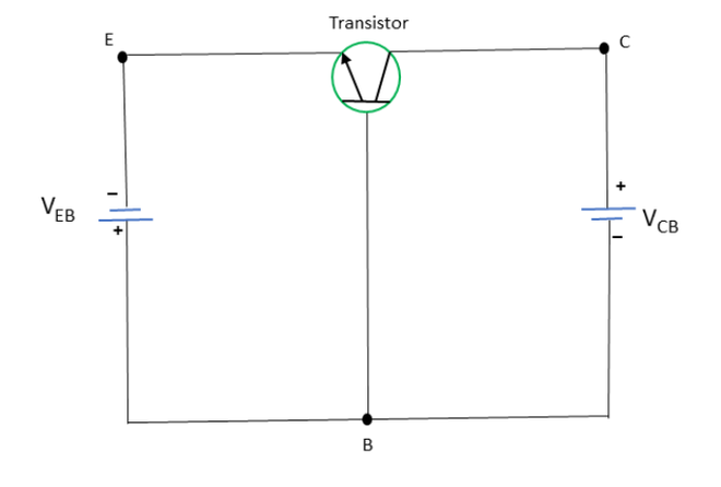
Active region
Voltage VEB is connected between emitter and base in a forward-biased manner and voltage VCB is connected between collector and base in a reverse-biased manner. When a transistor is in active region then it is mainly used for amplification. In this region, collector current depends upon base current.
Saturation region
This is a region of operation where emitter-base junction is forward-biased and collector-base junction is also forward-biased.

Saturation region
Voltage VEB is connected between emitter and base in a forward-biased manner and voltage VCB is connected between collector and base in a forward-biased manner. In this region, collector current becomes independent of the base current. When a transistor is in saturation region then it acts like a closed switch.
Cut-off region
This is a region of operation where emitter-base junction is reverse-biased and collector-base junction is reverse-biased.
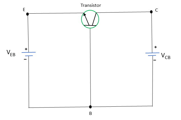
Cut-off region
Voltage VEB is connected between emitter and base in a reverse-biased manner and voltage VCB is connected between collector and base in a reverse-biased manner. In this region the value of current in the transistor is nearly zero. It is so because emitter does not emit ay charge carrier to base except few minority charge carriers which are generated thermally. When a transistor is in saturation region then it acts like an open switch.
Inverted region
This is a region of operation where emitter-base junction is reverse-biased and collector-base junction is forward-biased.

Inverted region
Voltage VEB is connected between emitter and base in a reverse-biased manner and voltage VCB is connected between collector and base in a forward-biased manner. In this region transistor is does not work properly. This region is not of much importance.
| Region of operation | Emitter-base junction | Collector-base junction |
|---|---|---|
| Active region | Forward-biased | Reverse-biased |
| Saturation region | Forward-biased | Forward-biased |
| Cut-off region | Reverse-biased | Reverse-biased |
| Inverted region | Reverse-biased | Forward-biased |
Advantages of transistors configuration
Advantages of different configurations of transistors are given below:
i. Common-Base Configuration:
Advantages of common-base configuration are given below:
* The common-base configuration has low input and output impedance which is used to drive loads of different impedances.
* This type of configuration offers low power consumption.
* The current gain(α) of this configuration is less affected by the change in temperature.
ii. Common-Emitter Configuration:
Advantages of common-emitter configuration are given below:
* Common-emitter configuration has high power gain which could be used when both current and voltage amplication is required.
* This type of configuration is easy to bias and therefore offers versality to various applications.
* Common-emitter configuration produces inverted output.
iii. Common-Collector Configuration:
Advantages of common-collector configuration are given below:
* This type of configuration has voltage gain close to unity which could be used for buffering of voltage.
* Common-collector configuration has high input impedance.
* There is no phase reversal between input signal and output signal.
Disadvantages of transistors configuration
Disadvantages of different configurations of transistors are listed below:
i. Common-Base Configuration:
Disadvantages of common-base configuration are given below:
* The output impedance of this configuration varies when there is change in applied load.
* Common-base configuration offers complex biasing of the circuit in comparison to other types of configurations.
* When input signal reaches power supply limits clipping of signal takes place.
ii. Common-Emitter Configuration:
Disadvantages of common-emitter configuration are given below:
* The output signal of common-emitter signal is inverted with respect to input signal.
* Common-emitter configuration is sensitive with variation in values of components.
* In this configuration a large amount of power is dissipated as heat and hence, are not power efficient.
iii. Common-Collector Configuration:
Disadvantages of common-collector configuration are given below:
* In common-collector configuration the value of input impedance changes with the connected load.
* There is a phase reversal between input and output signal in common-collector configuration.
* This configuration is temperature-sensitive, i.e., the parameters of circuit are affected by the change in temperature.
Applications of Transistor Configuration
Applications of different configurations of transistors are given below:
**Common-Base Configuration
Applications of common-base configuration are given below:
- It is commonly used in low-noise amplifiers.
- This type of configuration also finds their application in photodetectors to amplify the weak received signals.
- It is also used in frequency converters, i.e., it converts signals of one frequency to another.
Common-Emitter Configuration
Applications of common-base configuration are given below:
- These configurations are useful in voltage amplifiers.
- It also helps in modulation of received input signal.
- It is also useful in radio-frequency amplifiers.
Common-Collector Configuration
Applications of common-base configuration are given below:
- It is commonly used in voltage regulation.
- In RF applications it is used to match the impedance between different stages of a circuit.
- Common-collector configuration also finds their application in current buffers.
Comparison between CB, CE and CC configurations
| Characteristics | CE configuration | CB configuration | CC configuration |
|---|---|---|---|
| Input resistance | Low (50 KΩ) | Very low (40 Ω) | Very high (750 KΩ) |
| Output resistance | High (10 KΩ) | Very high (1 MΩ) | Low (50 Ω) |
| Current Gain | High (100) | Less than unity (0.98) | High (100) |
| Input voltage | Applied between base and emitter. | Applied between emitter and base. | Applied between base and collector. |
| Output voltage | Applied between `emitter and collector. | Applied between collector and emitter. | Applied between emitter and ground. |
| Leakage current | Very large. For Germanium 500 µA and for silicon 20 µA. | Very less. For Germanium 5 µA and for silicon 1 µA. | Very large. For Germanium 500 µA and for silicon 20 µA. |
| Voltage Gain | High (500) | Small (150) | Less than unity |
| Applications | Used in amplifier circuits. | Used for high-frequency applications. | Used for impedance matching. |
Conclusion
Thus, there are three different configurations in which three terminals of a bipolar junction transistor could be connected. The application of the transistor depends on the configuration of the transistor, as a bipolar junction transistor behaves differently in different configurations. All these configurations have certain characteristics and applications to make it desirable.