Capture Data over USB Ethernet - MATLAB & Simulink (original) (raw)
The FPGA data capture feature captures signal data from the FPGA and returns the data to MATLAB® or Simulink® over a JTAG, Ethernet (programmable logic (PL) Ethernet or processing system (PS) Ethernet), or universal serial bus (USB) Ethernet interface. Follow these instructions when you intend to capture data over a USB Ethernet interface. For other supported interfaces, follow the instructions in Data Capture Workflow.
Note
FPGA data capture supports the USB Ethernet interface for the AMD® Zynq® devices only.
- Set up hardware board
- Copy the compatible secure digital (SD) card image files for the hardware board to an SD card drive path. You can use the copyImageToHostSDCardPath or loadImageToTargetSDCardPath function to perform this step.
- Set the jumpers on the hardware board to configure the USB interface in peripheral mode.
- Connect the USB cable between the host computer and the target board.
- Set up host computer
- Windows® only — Install the USB Ethernet drivers.
- Configure the IP address of the USB Ethernet or RNDIS gadget in the host computer after the SD card is booted on the hardware board.
- Perform data capture operations
- Use the FPGA Data Capture Component Generator tool to configure and generate the data capture IP core. In the tool, set the Connection type parameter to
USB Ethernet. - Add the generated packaged IP core to the Vivado® user repository by using the addFPGADataCaptureToVivado function.
- Integrate the data capture IP into your Vivado design and connect the IP to the signals selected for data capture and specifying the triggers.
- Compile the modified FPGA design and generate the BIT file by using Vivado.
- Decompile your device tree blob (DTB) file by using the device tree compiler (DTC) tool and edit it to update the reserve memory nodes and LibIIO shared memory devices with respect to the data capture IP address mapping.
- Compile the updated DTB file by using the DTC tool.
- Use the loadBitstream function to load the BIT and DTB files based on your FPGA design.
- Use one of the following methods to capture data.
- Open the FPGA Data Capture tool. Set the trigger, capture condition, and data type parameters, and then capture data into the MATLAB workspace.
- Use the generated System object™ derived from hdlverifier.FPGADataReader. Set the data types, trigger condition, and capture condition using the methods and properties of the System object, and then call the object to capture data.
- In Simulink, open the generated model and configure the parameters of the FPGA Data Reader block. Then run the model to capture data.
- Use the FPGA Data Capture Component Generator tool to configure and generate the data capture IP core. In the tool, set the Connection type parameter to
The following sections describe the setup and data capture steps in detail. You can use theHardware Setup tool to automate the setup steps for the hardware board and host computer. For more information, see Guided Hardware Setup.
Complete Hardware Checklist
Confirm that you have all required hardware and accessories to complete the hardware setup.
- USB 3.0 or USB 2.0 cable — Use a USB 3.0 or USB 2.0 cable based on the type of USB cable your hardware board supports. This connection is necessary for transmitting data, such as a programming file, from the host computer to the hardware board. It is also necessary for sending and receiving signals to and from the hardware board.
Note
If you use a USB 2.0 cable for a board that supports USB 3.0, the cable throughputs lesser data. - SD card reader and writable SD card with a capacity of 4 GB or larger — If the host machine does not have an integrated card reader, use an external USB SD card reader.
- Supported hardware — You must have a supported hardware board. For the list of supported boards and interfaces, see Supported FPGA Devices for FPGA Verification. Do not connect or turn on the device until you are prompted at a later step.
- Power supply adapter, if the board requires one.
Set Up Hardware Board
Copy Image to SD Card in Host Computer
Copy the compatible SD card image files for the hardware board to an SD card drive path. This SD card image is included with the support package. The image includes the embedded software and the FPGA programming file necessary for using the hardware board as an I/O peripheral. If you have already copied the SD card with the required image, skip this step.
- Insert a 4 GB or larger SD card into the card reader on the host computer. The card must be in FAT32 format.

Note
Unlock the SD card before downloading the firmware image to the card. Keep the card unlocked while the card is in the card reader on the board. - Use the copyImageToHostSDCardPath function to copy the board-specific SD card image files to the specified SD card drive location in the host computer. The SD card image files contain a bootloader and supported operating system information. This function also copies the server daemon for handling the FPGA data capture host commands on the target hardware board.
If you use the Hardware Setup tool to set up your hardware board, this step is automated. See Select a Drive and Load Firmware.
Examples
This example copies a default SD card image to theG:drive location on the host computer for the ZCU102 board. Specify the IP address of the USB Ethernet gadget on the hardware board in dotted quad format followed byusb0/. This example sets the IP address of the USB Ethernet gadget on the ZCU102 board to192.168.3.2.
copyImageToHostSDCardPath('ZCU102','G:', ...
'DeviceAddress','usb0/192.168.3.2');
Update SD Card Image in Hardware Board (Optional)
If you have already copied the SD card image files by using the process in Copy Image to SD Card in Host Computer, skip this step.
Use the loadImageToTargetSDCardPath function to update the SD card image on the hardware board. Before proceeding with this step, make sure that the SD card is inserted in the target hardware board SD card location and that an Ethernet connection is established between the host computer and the target hardware board. This function uses the PS Ethernet connection to load the SD card image files.
The loadImageToTargetSDCardPath function updates the existing board-specific SD card image files on the hardware board. You might need to wait for at least 20 seconds for the SD card to update.
Examples
This example copies a default SD card image to the target hardware board SD card location for the ZCU102 board with the default PS Ethernet IP address 192.168.0.2. Specify the IP address of the USB Ethernet gadget on the hardware board in dotted quad format followed by usb0/. This example sets the IP address of the USB Ethernet gadget on the ZCU102 board to 192.168.3.2.
loadImageToTargetSDCardPath('ZCU102', ... 'DeviceAddress','usb0/192.168.3.2');
This example copies a default SD card image to the target hardware board SD card location for the ZCU102 board with the PS Ethernet IP address 192.168.5.2. The example sets the IP address of the USB Ethernet gadget on the hardware board to192.168.3.2.
loadImageToTargetSDCardPath('ZCU102', ... 'DeviceAddress',{'192.168.5.2','usb0/192.168.3.2'});
Set Jumper Switches
Set the jumpers on the hardware board to configure the USB cable in peripheral mode. Make sure that the board is turned off. The jumper settings are different for each board. To learn more about the settings, see the board documentation.
For example, set these jumper settings for the ZCU102 board.
Set Jumpers on ZCU102
Set SW6 and other jumpers to the values in this table. The SW6 jumper settings make sure that the board starts up from the SD card.
| SW6 Switch | SW6 Switch Position |
|---|---|
| 1 | Up |
| 2 | Down |
| 3 | Down |
| 4 | Down |

Set the J7, J113, J110, and J109 jumpers to the values in this table. These settings set up the hardware board so that it can communicate with the host computer over a USB Ethernet interface.
| Jumper | Jumper Position |
|---|---|
| J7 | Off |
| J113 | 1-2 |
| J110 | 1-2 |
| J109 | No jumper |

To know the jumper settings for the other supported boards, see Set Jumpers.
Set Up Host Computer
Install USB Ethernet Drivers
This step is required only for the Windows operating system.
You must install the USB Ethernet drivers before you use HDL Verifier™ features with a USB Ethernet connection. To install the drivers, in theHardware Setup tool, on the Install Drivers screen, click Install Driver. The installation process might require system administrator privileges.
Configure USB on Host Computer
You must configure the host computer so that it can communicate with the hardware board. After you boot the SD card on the target hardware board, the board appears as the MathWorks® USB Ethernet or RNDIS gadget on the host computer.
If you use the Hardware Setup tool, select the USB Ethernet or RNDIS gadget that you want to connect to the hardware board. For more information, see Configure USB on Host Computer. If you have already configured the USB Ethernet gadget, skip this step.
Note
The guided setup supports the USB configuration on the Windows operating system only. For the Linux® operating system, you must configure the USB Ethernet gadget manually.
By default, the RNDIS gadget on the host computer fetches the IP address from the dynamic host configuration protocol (DHCP) service running on the hardware board. To manually configure the host computer, follow the steps for your specific operating system.
Configure Windows. Follow these instructions for Windows 7 or later.
- From the Start menu, click Control Panel.
- Set View by to
Category. - Click Network and Internet.
- Click Network and Sharing Center.
- On the left pane, click Change adapter settings.

- Right-click the USB Ethernet connection that is connected to the hardware board and select Properties.
- On the Networking tab of the Properties dialog box, clear all options except Internet Protocol Version 4 (TCP/IPv4). Other services, particularly antivirus software, can cause intermittent connection problems with the hardware board.
- Double-click Internet Protocol Version 4 (TCP/IPv4).
- On the General tab, select Use the following IP address.
- The default IP address of the hardware board is
192.168.1.2. The host network connection must be on the same subnet as the hardware board. To meet this requirement, make sure to assign a compatible IP address to the host network connection. Set the host network IP address to 192.168.1.x, wherexis either 1 or an integer in the range [3, 255].
If the first three octets of the IP address field are not 192.168.1, then your hardware board is on another subnet. Enter the same subnet number in the IP address. - Leave the subnet mask set to the default value of
255.255.255.0. - Click OK.
Configure Linux. Set the host USB Ethernet interface to have a static IP address. This configuration enables communication with the hardware board. The default IP address of the hardware board is 192.168.1.2. The host network connection must be on the same subnet as the hardware board. To meet this requirement, you must assign a compatible IP address to the host network connection.
- Set the host network IP address to 192.168.1.
x, wherexis either 1 or an integer in the range [3, 255]. Set this value by using theifconfigcommand. For example, enter this command in the shell.
% sudo ifconfig usb_Z_ 192.168.1.4 netmask 255.255.255.0
In this syntax,usb_`Z`_is the name of the host USB port (usually usb_0_, usb_1_, and so on). To use thesudocommand, you might have to enter a password. - Confirm the changes by entering this command in the shell.
usb_`Z`_is the name of the host USB port you set in the previous step.
Perform Data Capture Operations
Configure and Generate Data Capture IP
Use the FPGA Data Capture Component Generator tool to configure and generate the data capture IPs. In the tool:
- Set FPGA vendor to
AMDandConnection type toUSB Ethernet. - Specify the port names and sizes for the data capture IP. These ports connect to the signals that you want to capture and the signals that you want to use as triggers for each capture.
- Select storage type as either internal memory or external memory. Internal memory uses internal BRAM resources to store captured data, while external memory uses external DDR memory connected to the FPGA for storage.
- Specify how many samples to return, maximum number of trigger stages, and whether to include capture condition logic for the data capture IP.
- Click Generate.
The tool generates these data capture components in the specified destination folder:
- Packaged IP core, for integration into your FPGA design. The IP core contains:
- A port for each signal you want to capture or use as part of a trigger condition.
- Memory to capture the number of samples you requested for each signal.
- An interface logic (AXI4 subordinate interface) to communicate with the processor.
- Trigger and capture condition logic that can be configured at run time.
- A ready-to-capture signal to control data flow from the FPGA.
- Generation report, with list of generated files and instructions for next steps.
- Tool to set capture parameters and capture data to the MATLAB workspace.
- Customized version of the data capture System object that provides an alternative, programmatic, way to configure and capture data.
- Simulink model that contains a customized FPGA Data Reader block. This model streams the captured signals into the Logic Analyzer waveform viewer. You can also use the Scope block to display the signals.
- MAT file in the
_`generatedIPName`__generation_settings.matformat, where_`generatedIPName`_is the name of the generated HDL IP core. This MAT file holds the data capture build parameters. To reload the same design in your next iteration, provide this MAT file as an input argument to thegenerateFPGADataCaptureIP function.
Add Data Capture IP to Vivado Project
Add the generated packaged IP core to the Vivado user repository by using the addFPGADataCaptureToVivado function.
- Create a Vivado project.
- Add the generated IP in the specified folder to the specified Vivado project.
addFPGADataCaptureToVivado("vivadoProjectPath",DataCaptureIPFolder="destinationFolder");_`vivadoProjectPath`_is the name of Vivado project location and_`destinationFolder`_is the name of the folder that contains the generated IP core.
For example, the following command adds the data capture IP in thehdlsrcfolder to theC:\test_design_zcu102\hdl_prj\vivado_ip_prj\vivado_prj.xprVivado project.
addFPGADataCaptureToVivado("C:\test_design_zcu102\hdl_prj\vivado_ip_prj\vivado_prj.xpr", ...
DataCaptureIPFolder="hdlsrc");
Integrate Data Capture IP into Vivado Design
To capture FPGA data, integrate the data capture IP into your Vivado design. To integrate the IP, follow the instructions in the generation report.
- Open the Vivado project. Then, open your block design and insert the data capture IP into it.
- Connect the subordinate AXI4 interface of the data capture IP to the manager AXI4 interface of the processor.

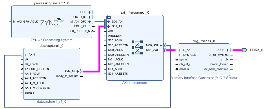
- External memory only — Connect the AXI4 manager (AXI4_M) interface of the data capture IP to the AXI4 subordinate (S_AXI) interface of MIG through AXI Interconnect, as this figure shows.
- Connect data capture IP to the signals you requested for capture and triggers.
- Complete the block design by connecting the
clk,clk_enable,IPCORE_RESETN,AXI4_ACLK, andAXI4_ARESETNinput ports of the data capture IP. Additionally, for external memory, connect theAXI4_M_ACLKandAXI4_M_ARESETNinput ports of the data capture IP. - External memory only — Make sure that the
AXI4_M_ACLK, used by the data capture IP to write data to external DDR memory, has a higher frequency than theclkclock.
Generate DTB File
Generate a DTB file for your hardware board by following these instructions.
- Log into the Linux operating system running on the target hardware board.
- Navigate to the
/mntpath. - Convert an existing DTB file into a corresponding human-readable device tree source (DTS) file by entering this command in the terminal.
dtc -I dtb -O dts devicetree_hdlv.dtb -o devicetree.dts
To generate a DTB file, you need a device tree compiler (DTC) on a Linux operating system. If a DTC is not installed, get the DTC source code and cross-compile to ARM®. - Open the converted DTS file by entering this command in the terminal.
- Edit the DTS file to update the reserve memory nodes and LibIIO shared memory devices with respect to the data capture IP address mapping.
Examples
The data capture IP address mapping in these examples consists of the following BRAM address region.Memory-Mapped Region Base Address Range BRAM — mw_axi_bram_ip0 0x40000000 0x200000 (2 MB)  Device-tree nodes for a 32-bit ARM Cortex-A9 based Zynq SoC devices
Update Reserve Memory Nodes This example reserves all BRAM memory to prevent Linux from using it and names it as reserved_region1./{ reserved-memory { #address-cells = <0x1>; #size-cells = <0x1>; ranges; linux,phandle = <0x39>; phandle = <0x39>; region1: region1@40000000 { reg = <0x40000000 0x200000>; no-map; }; }; }; Update LibIIO Shared Memory Devices This example inserts the mwipcoredriver into thefpga_axinodes. In this example, you must set themathworks,dev-nameproperty of the shared memory read and write channels to"rd0"and"wr0", respectively.&fpga_axi {
mwipcore@0 {
compatible = "mathworks,mwipcore-v3.00";
reg = <0x40010000 0x10000>;
#address-cells = <0x1>;
#size-cells = <0x0>;
sharedmem@0 {
#address-cells = <0x1>;
#size-cells = <0x0>;
reg = <0x0>;
compatible = "mathworks,sharedmem-v1.00";
memory-region = <®ion1>;
mathworks,dev-name = "mw_datacapture_bram_ip";
read-channel@0 {
reg = <0x0>;
compatible = "mathworks,sharedmem-read-channel-v1.00";
mathworks,dev-name = "rd0";
};
write-channel@1 {
reg = <0x1>;
compatible = "mathworks,sharedmem-write-channel-v1.00";
mathworks,dev-name = "wr0";
};
}; };
};![]() Device-tree nodes for a 64-bit ARM Cortex-A53 based MPSoC devices
Device-tree nodes for a 64-bit ARM Cortex-A53 based MPSoC devices
Update Reserve Memory Nodes
This example reserves all BRAM memory to prevent Linux from using it and names it as reserved_region1.
/{
reserved-memory {
#address-cells = <0x2>;
#size-cells = <0x2>;
ranges;
linux,phandle = <0x39>;
phandle = <0x39>;
region1: region1@40000000 {
reg = <0x0 0x40000000 0x0 0x200000>;
no-map;
};
};
};
Update LibIIO Shared Memory Devices
This example inserts the mwipcore driver into the fpga_axi nodes. In this example, you must set the mathworks,dev-name property of the shared memory read and write channels to "rd0" and "wr0", respectively.
&fpga_axi {
mwipcore@0 {
compatible = "mathworks,mwipcore-v3.00";
reg = <0x40010000 0x10000>;
#address-cells = <0x1>;
#size-cells = <0x0>;
sharedmem@0 {
#address-cells = <0x1>;
#size-cells = <0x0>;
reg = <0x0>;
compatible = "mathworks,sharedmem-v1.00";
memory-region = <®ion1>;
mathworks,dev-name = "mw_datacapture_bram_ip";
read-channel@0 {
reg = <0x0>;
compatible = "mathworks,sharedmem-read-channel-v1.00";
mathworks,dev-name = "rd0";
};
write-channel@1 {
reg = <0x1>;
compatible = "mathworks,sharedmem-write-channel-v1.00";
mathworks,dev-name = "wr0";
};
}; };
};
You can also compile a DTB file and edit a DTS file on the host Linux computer, but it gives a few warnings during compilation. You can ignore such warnings.
6. After you edit the DTS file, to generate a DTB file, enter this command in the terminal.
dtc -I dts -O dtb devicetree.dts -o devicetree_sharedmem_iio.dtb
You can now load this modified DTB file to the target hardware board. Use the loadBitstream function to load the custom FPGA bitstream and DTB files.
Load Bitstream File to Hardware Board
Use the loadBitstream function only if you have a new FPGA design to load on the target hardware board. Otherwise, skip this step.
This function loads the custom FPGA bitstream file and its corresponding DTB file to the target hardware board. You might need to wait for at least 20 seconds for the target hardware board to reflect your changes.
This example loads a custom FPGA bitstream and its corresponding DTB file to the ZCU102 board with a USB Ethernet IP address that is different from the default value.
loadBitstream('ZCU102','design.bit', ... 'devicetree.dtb', ... 'DeviceAddress','192.168.3.2');
When the program is running on your hardware board, you can communicate with the board.
Capture Data
The FPGA data capture IP core communicates over the USB cable between your FPGA board and the host computer. Make sure that the USB cable is connected. Before capturing data, you can set data types for the captured data, set a trigger condition that specifies when to capture the data, and set a capture condition that specifies the data to be captured. To configure these options and capture data, you can:
- Open the FPGA Data Capture tool. Set the trigger, capture condition, and data type parameters, and then capture data into the MATLAB workspace.
- Use the generated System object derived from hdlverifier.FPGADataReader. Set the data types, trigger condition, and capture condition using the methods and properties of the System object, and then call the object to capture data.
- In Simulink, open the generated model and configure the parameters of the FPGA Data Reader block. Then, run the model to capture data.
Set Base Address of External DDR Memory (for External Memory Only)
For external memory storage type, set the base address of the external DDR memory. To do this, use the MemoryBaseAddress property of the hdlverifier.FPGADataReader System object before capturing data to MATLAB. Set the External DDR memory base address parameter of the FPGA Data Reader block before capturing data to Simulink.
For example, the following command sets the base address of the DDR memory for thedatacapture1 System object to 80000000.
datacapture1.MemoryBaseAddress = "80000000";
Set Base Address of Data Capture IP and IP Address of Hardware Board
Set the base address of the data capture IP and the IP address of the target hardware board. To do this, use the CaptureBaseAddress and DeviceAddress properties of the hdlverifier.FPGADataReader System object before capturing data to MATLAB. Set the Device IP address and Data Capture IP core base address parameters of the FPGA Data Reader block before capturing data to Simulink.
For example, the following commands set the base address of thedatacapture1 data capture IP to 40000000 and the IP address of the target hardware board to 192.168.5.2.
datacapture1.CaptureBaseAddress = "40000000"; datacapture1.DeviceAddress = "192.168.5.2";
After you capture the data and import it into the MATLAB workspace or Simulink model, you can analyze, verify, and display the data.