Last Minute Notes Computer Organization (original) (raw)
Last Updated : 26 Dec, 2025
Computer architecture defines how a computer’s components communicate through electronic signals to perform input, processing, and output operations.
- It covers the design and organization of the CPU, memory, storage, and input/output devices.
- Describes how these components interact through buses, control signals, and data pathways.
- It directly influences the overall speed, functionality, and reliability of a computer system.
Basic Terminology
- **Control Unit - A control unit (CU) handles all processor control signals. It directs all input and output flow, fetches the code for instructions and controls how data moves around the system.
- **Arithmetic and Logic Unit (ALU) - The arithmetic logic unit is that part of the CPU that handles all the calculations the CPU may need, e.g. Addition, Subtraction, Comparisons. It performs Logical Operations, Bit Shifting Operations, and Arithmetic Operation.
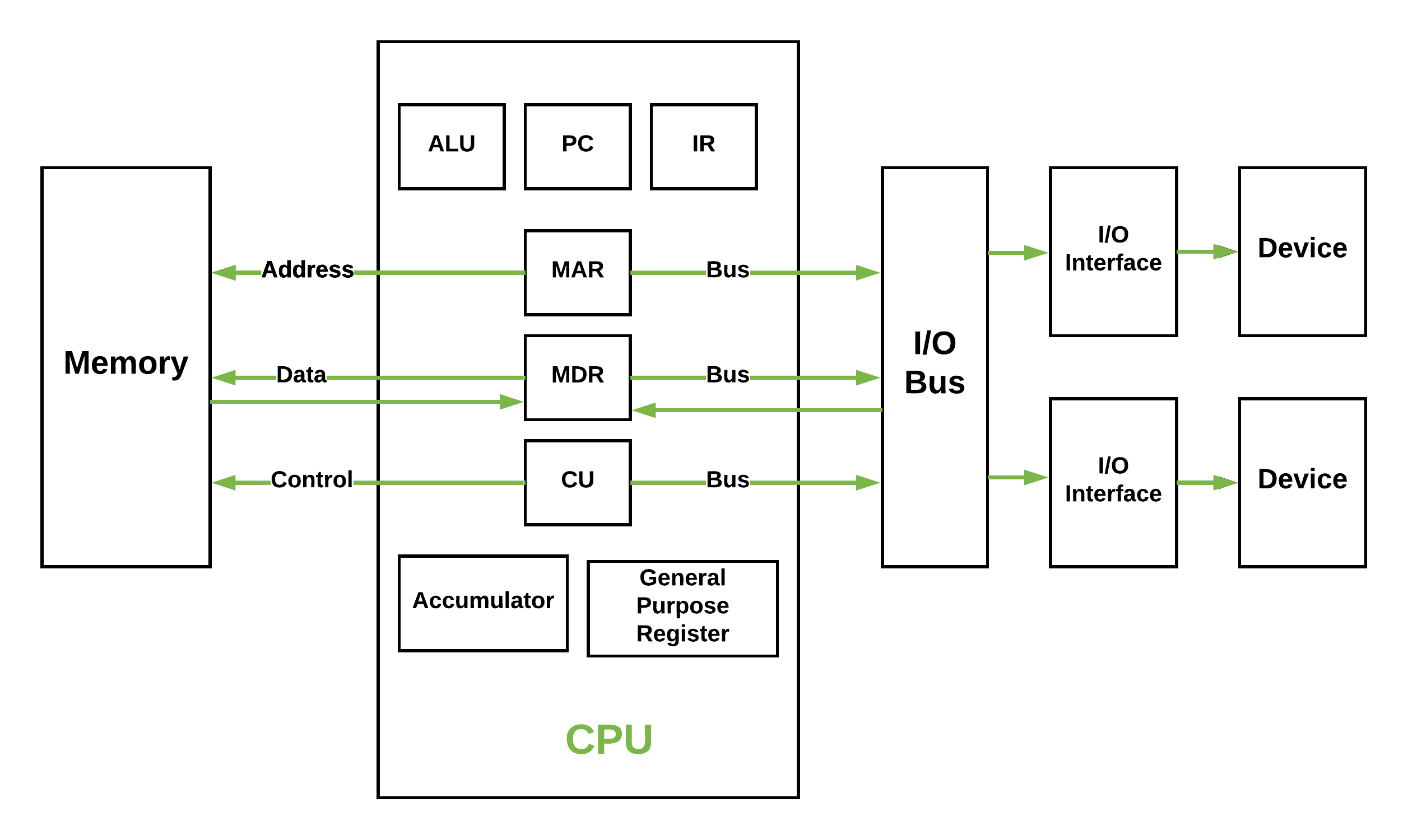 **Figure - Basic CPU structure, illustrating ALU
- **Main Memory Unit (Registers) -
- **Accumulator: Stores the results of calculations made by ALU.
- **Program Counter (PC): Keeps track of the memory location of the next instructions to be dealt with. The PC then passes this next address to Memory Address Register (MAR).
- **Memory Address Register (MAR): It stores the memory locations of instructions that need to be fetched from memory or stored into memory.
- **Memory Data Register (MDR): It stores instructions fetched from memory or any data that is to be transferred to, and stored in, memory.
- **Current Instruction Register (CIR): It stores the most recently fetched instructions while it is waiting to be coded and executed.
- **Instruction Buffer Register (IBR): The instruction that is not to be executed immediately is placed in the instruction buffer register IBR.
- **Input/Output Devices - Program or data is read into main memory from the _input device or secondary storage under the control of CPU input instruction. _Output devices are used to output the information from a computer.
- **Buses - Data is transmitted from one part of a computer to another, connecting all major internal components to the CPU and memory, by the means of Buses. Types:
- **Data Bus: It carries data among the memory unit, the I/O devices, and the processor.
- **Address Bus: It carries the address of data (not the actual data) between memory and processor.
- **Control Bus: It carries control commands from the CPU (and status signals from other devices) in order to control and coordinate all the activities within the computer.
Types of Computer Architecture
**1. **Von Neumann Architecture
- It uses one memory to store both the program instructions and the data.
- The CPU fetches instructions and data from the same place, one after another.
- This design is simpler and used in most traditional computers.
**2. **Harvard Architecture
- It uses two separate memories: one for program instructions and another for data.
- The CPU can fetch instructions and data at the same time, making it faster.
- This design is used in modern systems like embedded processors.
Instruction Set and Addressing Modes
Instruction Formats (Zero, One, Two and Three Address Instruction)
A instruction is of various length depending upon the number of addresses it contain. Generally CPU organization are of three types on the basis of number of address fields:
- Single Accumulator organization
- General register organization
- Stack organization
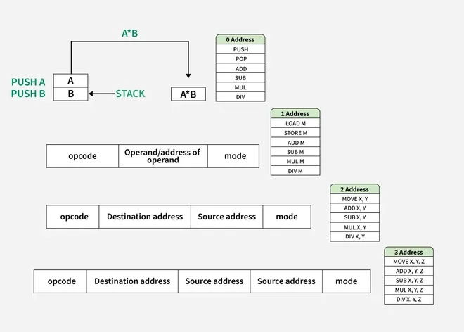
Read more about Instruction Format, Here.
**Basic Machine Instructions in COA
Machine instructions are the basic commands given to the processor to perform tasks. They operate directly on the hardware.
**Types of Machine Instructions
**Data Transfer Instructions
- Move data between memory, registers, or I/O devices.
- Example:
LOAD,STORE,MOVE.
**Arithmetic Instructions
- Perform arithmetic operations like addition, subtraction, multiplication, and division.
- Example:
ADD,SUB,MUL,DIV.
**Logical Instructions
- Perform logical operations such as AND, OR, NOT, XOR.
- Example:
AND,OR,NOT,XOR.
**Control Transfer Instructions
- Change the sequence of execution (jump, branch, or call).
- Example:
JUMP,CALL,RET.
**Input/Output Instructions
- Allow communication between the processor and external devices.
- Example:
IN,OUT.
**Shift and Rotate Instructions
- Shift or rotate bits in a register.
- Example:
SHL(Shift Left),SHR(Shift Right),ROL(Rotate Left),ROR(Rotate Right).
**Components of an Instruction
- **Opcode: Specifies the operation to perform (e.g., ADD, SUB).
- **Operands: Data to be operated on (e.g., registers, memory locations).
Addressing Modes
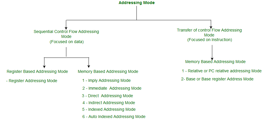
The addressing mode specifies a rule for interpreting or modifying the address field of the instruction before the operand is actually executed. An assembly language program instruction consists of two parts :

| **Addressing Mode | **Description | **Example |
|---|---|---|
| **Immediate Addressing | The operand is directly given in the instruction. | ADD R1, 5 (Add 5 to R1) |
| **Register Addressing | The operand is stored in a register. | ADD R1, R2 (Add R2 to R1) |
| **Direct Addressing | The operand is in memory, and the memory address is specified directly in the instruction. | LOAD R1, 1000 (Load data from memory address 1000 into R1) |
| **Indirect Addressing | The address of the operand is stored in a register or memory location, not directly in the instruction. | LOAD R1, (R2) (Load data from the memory address stored in R2 into R1) |
| **Register Indirect | Similar to indirect addressing, but specifically uses registers to hold the address of the operand. | LOAD R1, (R3) (Use R3 as pointer) |
| **Indexed Addressing | The operand's address is calculated by adding an index (offset) to a base address stored in a register. | LOAD R1, 1000(R2) (Load data from memory address 1000 + R2 into R1) |
| **Base Addressing | The base address is stored in a register, and the operand's offset is specified in the instruction. | LOAD R1, 200(RB) (RB = Base Register) |
| **Relative Addressing | The operand's address is determined by adding an offset to the current program counter (PC). | JUMP 200 (Jump to PC + 200) |
| **Implicit Addressing | The operand is implied by the instruction itself (no explicit address or operand). | CLR (Clear accumulator) |
**Effective address or Offset: An offset is determined by adding any combination of three address elements: displacement, base and index.
Read more about Addressing Modes, Here.
RISC vs CISC
| RISC | CISC |
|---|---|
| Focus on software | Focus on hardware |
| Uses only Hardwired control unit | Uses both hardwired and microprogrammed control unit |
| Transistors are used for more registers | Transistors are used for storing complexInstructions |
| Fixed sized instructions | Variable sized instructions |
| Can perform only Register to Register Arithmetic operations | Can perform REG to REG or REG to MEM or MEM to MEM |
| Requires more number of registers | Requires less number of registers |
| Code size is large | Code size is small |
| An instruction executed in a single clock cycle | Instruction takes more than one clock cycle |
| An instruction fit in one word. | Instructions are larger than the size of one word |
| Simple and limited addressing modes. | Complex and more addressing modes. |
| RISC is Reduced Instruction Cycle. | CISC is Complex Instruction Cycle. |
| The number of instructions are less as compared to CISC. | The number of instructions are more as compared to RISC. |
| It consumes the low power. | It consumes more/high power. |
| RISC is highly pipelined. | CISC is less pipelined. |
| RISC required more RAM . | CISC required less RAM. |
| Here, Addressing modes are less. | Here, Addressing modes are more. |
Read more about RISC vs CISC, Here.
Instruction Design and Format
CPU Registers
The instruction cycle involves multiple registers in the CPU to fetch, decode, execute and store results.
**Program Counter (PC)
- Holds the address of the next instruction to be executed.
- Updates after each instruction fetch.
**Instruction Register (IR)
- Stores the currently fetched instruction.
- Used by the control unit for decoding.
**Memory Address Register (MAR)
- Holds the memory address of the data or instruction to be fetched or stored.
**Memory Data Register (MDR) (or **Memory Buffer Register, MBR)
- Temporarily holds the data being transferred to/from memory.
**Accumulator (AC)
- Stores intermediate arithmetic and logic results during execution.
**General Purpose Registers (GPR)
- Temporary storage for operands, results, or data during execution.
**Temporary Register (TR)
- Stores intermediate data during complex operations or instruction execution.
**Status Register / Flag Register
- Stores condition flags (e.g., zero, carry, overflow) to indicate the result of operations.
**Stack Pointer (SP)
- Points to the top of the stack in memory, used during function calls or interrupts.

Flag Registers
**Status Flags
- **Zero Flag (Z): When an arithmetic operation results in zero, the flip-flop called the Zero flag - which is set to one.
- **Carry flag (CY): After an addition of two numbers, if the sum in the accumulator is larger than eight bits, then the flip-flop uses to indicate a carry called the Carry flag, which is set to one.
- **Parity (P): If the result has an even number of 1s, the flag is set to 1; for an odd number of 1s the flag is reset.
- **Auxiliary Carry (AC): In an arithmetic operation, when a carry is generated from lower nibble and passed on to higher nibble then this register is set to 1.
- **Sign flag(S): It is a single bit in a system status (flag) register used to indicate whether the result of the last mathematical operation resulted in a value in which the most significant bit was set.
Instruction Cycle
**1. Fetch: The CPU retrieves the next instruction from memory using the Program Counter (PC).
**2. Indirect: If the instruction uses an **indirect addressing mode, the effective memory address of the operand is resolved. Example: For LOAD R1, (100), the CPU fetches the address stored at memory location 100.
**3. Execute: The CPU performs the operation specified by the instruction (e.g., arithmetic, logical, control).
**4. Interrupt: If an interrupt request occurs (e.g., hardware interrupt or software exception), the CPU temporarily halts the current execution to service the interrupt. After servicing, the CPU resumes the instruction cycle.
**Standard Instruction Cycle
This includes the basic steps for executing instructions:
- **Fetch: Retrieve the instruction from memory.
- **Decode: Identify the operation and operands.
- **Execute: Perform the operation.
- **Store (Write Back): Save the result (if any).
Read more about Instruction Cycle, Here.
Control Unit
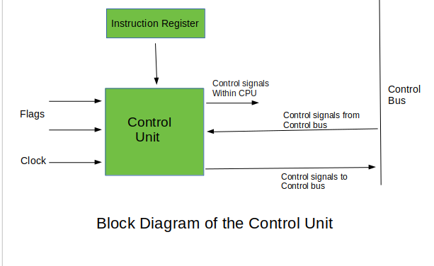
The Control Unit (CU) is a core component of the CPU that directs its operation by generating control signals. It manages the execution of instructions by coordinating with the ALU, registers, and memory.
**Types of Control Units
**Hardwired Control Unit -
- Fixed logic circuits that correspond directly to the Boolean expressions are used to generate the control signals.
- Hardwired control is faster than micro-programmed control.
- A controller that uses this approach can operate at high speed.
- RISC architecture is based on hardwired control unit.
**Micro-programmed Control Unit -
- The control signals associated with operations are stored in special memory units inaccessible by the programmer as Control Words.
- Control signals are generated by a program are similar to machine language programs.
- Micro-programmed control unit is slower in speed because of the time it takes to fetch microinstructions from the control memory.
There are two type Micro-programmed control Unit:
- **Horizontal Micro-programmed control Unit- The control signals are represented in the decoded binary format that is 1 bit/CS.
- **Vertical Micro-programmed control Unit - The control signals re represented in the encoded binary format. For N control signals- Logn(N) bits are required.
Read more about Hardwired CU vs Micro-programmed CU, Here.
**Microprogram: Program stored in memory that generates all control signals required to execute the instruction set correctly, it consists micro-instructions.
**Micro-instruction: Contains a sequencing word and a control word. The control word is all control information required for one clock cycle.
**Micro-operations: Micro-operations are the atomic operations which executes a particular micro-instruction. Example of micro-operation during the fetch cycle:
t1: MAR ←(PC)
t2: MBR ←Memory
PC ←(PC) + I
t3: IR ←(MBR)
Memory Organization
- Memories are made up of registers.
- Each register in the memory is one storage location.
- The storage location is also called a memory location.
- Memory locations are identified using Address.
- The total number of bit a memory can store is its capacity.
| Byte Addressable Memory | Word Addressable Memory |
|---|---|
| When the _data space in the cell = 8 bits then the corresponding _address space is called as Byte Address. | When the _data space in the cell = word length of CPU then the corresponding _address space is called as Word Address. |
| Based on this data storage i.e. _Bytewise storage, the memory chip configuration is named as **Byte Addressable Memory. | Based on this data storage i.e. _Wordwise storage, the memory chip configuration is named as **Word Addressable Memory. |
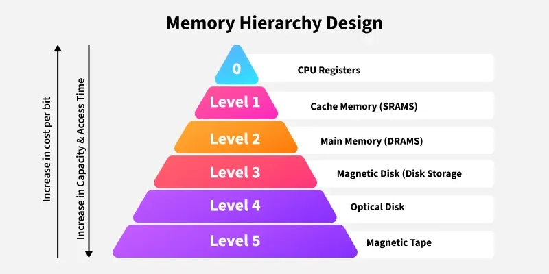
Memory Hierarchy
**Simultaneous access memory organization: If H1 and H2 are the Hit Ratios and T1 and T2 are the access time of L1 and L2 memory levels respectively then the
_Average Memory Access Time can be calculated as:
T=(H1*T1)+((1-H1)*H2*T2
**Hierarchical Access Memory Organization: If H1 and H2 are the Hit Ratios and T1 and T2 are the access time of L1 and L2 memory levels respectively then
_Average Memory Access Time can be calculated as:
T=(H1*T1)+((1-H1)*H2*(T1+T2)
Read more about Simultaneous and Hierarchical Access Memory Organization, Here.
Cache Memory
Cache Memory is a special very high-speed memory. It is used to speed up and synchronizing with high-speed CPU. Levels of memory: Level 1 or Register, Level 2 or Cache memory, Level 3 or Main Memory, Level 4 or Secondary Memory.
Hit ratio = hit / (hit + miss) = no. of hits/total accesses
**Locality of reference - Since size of cache memory is less as compared to main memory. So to check which part of main memory should be given priority and loaded in the cache is decided based on the locality of reference.
**Types of Locality of reference
- **Spatial Locality of reference: Spatial locality means instruction or data near to the current memory location that is being fetched, may be needed soon in the near future.
- **Temporal Locality of reference: Temporal locality means current data or instruction that is being fetched may be needed soon. So we should store that data or instruction in the cache memory to avoid searching again in main memory for the same data.
- **Cache Mapping: There are three different types of mapping used for the purpose of cache memory which is as follows: Direct mapping, Associative mapping and Set-Associative mapping.
**Direct Mapping - Maps each block of main memory into only one possible cache line. If a line is previously taken up by a memory block and a new block needs to be loaded, the old block is trashed. An address space is split into two parts index field and a tag field. The cache is used to store the tag field whereas the rest is stored in the main memory.
**Cache Line Number = Main Memory block Number % Number of Blocks in Cache
**Associative Mapping - A block of main memory can map to any line of the cache that is freely available at that moment. The word offset bits are used to identify which word in the block is needed, all of the remaining bits become Tag.
**Set-Associative Mapping - Cache lines are grouped into sets where each set contains k number of lines and a particular block of main memory can map to only one particular set of the cache. However, within that set, the memory block can map to any freely available cache line.
**Cache Set Number = Main Memory block number % Number of sets in cache
Note: Translation Lookaside Buffer (i.e. TLB) is required only if Virtual Memory is used by a processor. In short, TLB speeds up the translation of virtual address to a physical address by storing page-table in faster memory. In fact, TLB also sits between the CPU and Main memory.
Read more about Cache Mapping Techniques, Here.
**Multilevel Cache
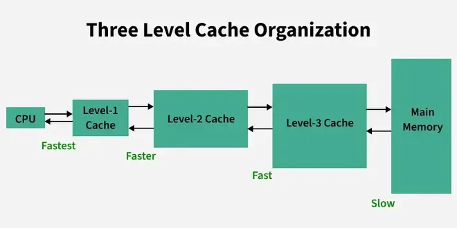
Multilevel Cache
Multilevel Caching is used in modern processors to improve memory access speed by introducing multiple levels of cache memory.
**Types of Cache Levels
**L1 Cache (Level 1):
- Smallest, fastest, and closest to the CPU.
- Usually divided into Instruction Cache and Data Cache.
**L2 Cache (Level 2):
- Larger and slower than L1 but still faster than main memory.
- Acts as a bridge between L1 and L3/main memory.
**L3 Cache (Level 3):
- Shared across multiple cores.
- Larger and slower than L2 but faster than main memory.
**Performance Metrics
- **Hit Ratio:Percentage of memory accesses satisfied by the cache. \text{Hit Ratio} = \frac{\text{Cache Hits}}{\text{Total Accesses}}
- **Miss Ratio: Percentage of memory accesses that result in a miss. \text{Miss Ratio} = 1 - \text{Hit Ratio}**Effective Memory Access Time (EMAT)
For **2-level cache:
\text{EMAT} = H_1 \times T_1 + (1 - H_1) \times [H_2 \times T_2 + (1 - H_2) \times T_M]- H1,H2H_1, H_2: Hit ratios for L1 and L2 caches.
- T1,T2T_1, T_2: Access times for L1 and L2 caches.
- TMT_M: Access time for main memory.
Cache Replacement Policies Table
| **Algorithm | **Key Idea |
|---|---|
| **LRU | Replace least recently used block |
| **FIFO | Replace oldest block |
| **Random | Replace random block |
| **LFU | Replace least-used block |
| **Optimal | Replace block not used longest |
Cache Updation Policy
**Write Through: In this technique, all write operations are made to main memory as well as to the cache, ensuring that main memory is always valid.
For hierarchical access: T_{read} = H \times T_{cache} + (1-H) \times (T_{cache} + T_{memory\_block}) \newline= T_{cache} + (1-H) \times T_{memory\_block}
For simultaneous access : T_{read} = H \times T_{cache} + (1-H) \times (T_{memory\_block}) \newlineT_{write} = T_{memory\_word}
**Write Back: In write-back updates are made only in the cache. When an update occurs, a dirty bit, or use bit, associated with the line is set. Then, when a block is replaced, it is written back to main memory if and only if the dirty bit is set.
For hierarchical access: T_{read} = T_{write} = H \times T_{cache} + (1-H) \times (T_{cache} + T_{memory\_block} + T_{write\_back}) \\= T_{cache} + (1-H) \times (T_{memory\_block} + T_{write\_back}), \\ \text{ where } T_{write\_back} = x \times T_{memory\_block}, \text{ where } x \text{ is the fraction of dirty blocks}
For simultaneous access : T_{read} = T_{write} = H \times T_{cache} + (1-H) \times ( T_{memory\_block} + T_{write\_back}), \\ \text{ where } T_{write\_back} = x \times T_{memory\_block}, \text{ where } x \text{ is the fraction of dirty blocks}
Read more about Cache Memory, Here****.**
**Cache Miss
| **Type of Miss | **Reason |
|---|---|
| **Compulsory Miss | First-time access to data |
| **Conflict Miss | Multiple blocks mapped to same cache line |
| **Capacity Miss | Cache cannot hold all required data |
Read about Types of Cache Miss, Here.
I/O Interface
- An I/O (Input/Output) Interface connects the CPU and memory with external devices like keyboards, monitors, printers, etc.
- It acts as a bridge between the CPU and I/O devices to ensure smooth data transfer.
Data transfer between the main memory and I/o device may be handled in a variety of modes like :
**Programmed I/O: In Programmed I/O, the CPU controls data transfer between the I/O device and memory without allowing direct access for the device. The I/O device sends one byte at a time, placing the data on the I/O bus and enabling the data valid line. The interface stores the byte in its data register, activates the data accepted line, and sets a flag bit to notify the CPU. The I/O device waits for the data accepted line to reset before sending the next byte. This process is managed step-by-step by the CPU, making it slower but synchronized.
**Interrupt driven I/O: In interrupt driven I/O, the processor issues an I/O command, continues to execute other instructions, and is interrupted by the I/O module when the I/O module completes its work.
Read more about Interrupt, Here.
**Interrupt Handling Techniques
- **Daisy Chaining in Interrupts
Daisy chaining is a method of handling multiple interrupts in a system by connecting the devices in a serial or chain-like manner. When an interrupt request is generated, the priority is determined by the position of the device in the chain. The device closer to the CPU has higher priority. The interrupt signal travels through the chain, and each device checks if it is the source of the interrupt. If not, it passes the signal to the next device in the chain. This approach is simple to implement but suffers from longer delays for devices farther down the chain and is unsuitable for systems requiring precise or equal priority handling.
- **Parallel Priority Interrupt
Parallel priority interrupts use a priority encoder to handle multiple interrupt requests simultaneously. All devices send their interrupt requests in parallel to the encoder, which determines the highest-priority interrupt and sends it to the CPU. This method is faster and more efficient than daisy chaining because it does not rely on signal propagation through a chain. Each device is assigned a priority, and the encoder ensures that the device with the highest priority gets serviced first. Parallel priority interrupts are commonly used in systems where speed and fair priority handling are essential.
**Direct Memory Access(DMA): In Direct Memory Access (DMA), the I/O module and main memory exchange data directly without processor involvement.
**Modes of DMA Transfer
**1. Burst Mode (Block Transfer Mode)
In burst mode, the DMA controller takes full control of the system bus and transfers an entire block of data in one go before releasing the bus back to the CPU. This method is fast but can cause the CPU to be idle during the transfer, as it doesn't get access to the bus until the transfer is complete.
**2. Cycle Stealing Mode
In cycle stealing mode, the DMA controller takes control of the bus for one data transfer (one word or one byte) at a time and then releases it back to the CPU. This allows the CPU and DMA to share the bus alternately, improving overall system efficiency while slightly slowing the DMA transfer.
Read more about Modes of DMA Transfer, Here.
| **Mode | **Key Feature | **CPU Involvement | **Use Case |
|---|---|---|---|
| **Programmed I/O | CPU waits for device (polling) | High | Slow devices |
| **Interrupt I/O | Device signals CPU via interrupt | Medium | Keyboards, printers |
| **DMA | DMA controller handles transfer | Low (only initiation) | High-speed or bulk data devices |
**DMA Controller
The DMA (Direct Memory Access) Controller is a hardware component that manages data transfer between memory and I/O devices without constant CPU involvement. It communicates with the CPU, memory, and I/O devices through control and data lines.
The CPU interacts with the DMA controller by selecting its registers via the address bus while enabling the DS (Data Select) and RS (Register Select) inputs. When the CPU grants the bus to the DMA (indicated by BG = 1, Bus Grant), the DMA takes control of the buses. The DMA then directly communicates with memory by placing the memory address on the address bus and activating the RD (Read) or WR (Write) control signals to perform data transfer.
The DMA controller communicates with external I/O devices using request and acknowledge lines:
- The I/O device sends a request signal when it needs to transfer data.
- The DMA acknowledges this request, initiates the data transfer, and ensures synchronization.
This process enables efficient and high-speed data transfer while freeing the CPU to perform other tasks.
Read more about I/O Interface, Here.
Pipelining
- Pipelining is a process of arrangement of hardware elements of the CPU such that its overall performance is increased.
- Simultaneous execution of more than one instruction takes place in a pipelined processor.
- RISC processor has 5 stage instruction pipeline to execute all the instructions in the RISC instruction set. Following are the 5 stages of RISC pipeline with their respective operations:
- **Stage 1 (Instruction Fetch) In this stage the CPU reads instructions from the address in the memory whose value is present in the program counter.
- **Stage 2 (Instruction Decode) In this stage, instruction is decoded and the register file is accessed to get the values from the registers used in the instruction.
- **Stage 3 (Instruction Execute) In this stage, ALU operations are performed.
- **Stage 4 (Memory Access) In this stage, memory operands are read and written from/to the memory that is present in the instruction.
- **Stage 5 (Write Back) In this stage, computed/fetched value is written back to the register present in the instructions.
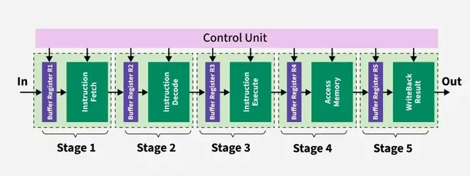
5 stages of pipeline
**Performance of a pipelined processor
Consider a 'k' segment/stages pipeline with clock cycle time as 'Tp'. Let there be 'n' tasks to be completed in the pipelined processor. So, time taken to execute 'n' instructions in a pipelined processor:
ETpipeline = k + n – 1 cycles
= (k + n – 1) Tp
In the same case, for a non-pipelined processor, execution time of 'n' instructions will be:
ETnon-pipeline = n * k * Tp
So, speedup (S) of the pipelined processor over non-pipelined processor, when 'n' tasks are executed on the same processor is:
S = Performance of pipelined processor / Performance of Non-pipelined processor
As the performance of a processor is inversely proportional to the execution time, we have:
S = ETnon-pipeline / ETpipeline
=> S = [n * k * Tp] / [(k + n – 1) * Tp]
S = [n * k] / [k + n – 1]
When the number of tasks 'n' are significantly larger than k, that is, n >> k
S = n * k / n
S = k
where 'k' are the number of stages in the pipeline. Also,
**Efficiency = Given speed up / Max speed up = S / Smax
We know that, Smax = k So,
**Efficiency = S / k
**Throughput = Number of instructions / Total time to complete the instructions So,
**Throughput = n / (k + n – 1) * Tp
Note: The cycles per instruction (CPI) value of an ideal pipelined processor is 1
**Performance of pipeline with stalls
**Speed Up (S) = CPI non-pipeline / (1 + Number of stalls per instruction)
Read more about Pipelining, Here.
**Dependencies and Data Hazard
There are mainly three types of dependencies possible in a pipelined processor. These are :
**Structural dependency:
- This dependency arises due to the resource conflict in the pipeline. A resource conflict is a situation when more than one instruction tries to access the same resource in the same cycle. A resource can be a register, memory, or ALU.
- To minimize structural dependency stalls in the pipeline, we use a hardware mechanism called Renaming.
**Control Dependency:
- This type of dependency occurs during the transfer of control instructions such as BRANCH, CALL, JMP, etc. On many instruction architectures, the processor will not know the target address of these instructions when it needs to insert the new instruction into the pipeline. Due to this, unwanted instructions are fed to the pipeline.
- Branch Prediction is the method through which stalls due to control dependency can be eliminated. In this at 1st stage prediction is done about which branch will be taken.
**Data Dependency :
- Data dependency occurs when one instruction depends on the result of another instruction. It can cause data hazards in pipelined processors.
**Types of Hazards in Pipelined Processors
Hazards are situations that cause the pipeline to stall or delay instruction execution. There are three main types of hazards:
1. **Structural Hazards
- Occur when hardware resources are insufficient to handle the current instruction stream.
- Example: If only one memory unit exists, and both instruction fetch and data access need it simultaneously.
**Solution:
- Add more resources (e.g., separate instruction and data memory – Harvard architecture).
- Use scheduling to avoid conflicts.
2. **Data Hazards
- Arise when an instruction depends on data from a previous instruction that has not yet completed.
**Types of Data Hazards:
- **RAW (Read After Write): True dependency.
- **WAR (Write After Read): Anti-dependency.
- **WAW (Write After Write): Output dependency.
**Solution:
- Data forwarding/bypassing.
- Insert pipeline stalls (NOPs).
- Instruction scheduling.
3. **Control Hazards
- Occur due to branch or jump instructions, where the next instruction to execute is uncertain until the branch is resolved.
**Solution:
- Branch prediction techniques.
- Delayed branching (use NOPs).
- Dynamic scheduling.
Read more about Dependencies and Hazards, Here.
IEEE Standard 754 Floating Point Numbers
There are several ways to represent floating point number but IEEE 754 is the most efficient in most cases. IEEE 754 has 3 basic components:
**The Sign of Mantissa - This is as simple as the name. 0 represents a positive number while 1 represents a negative number.
**The Biased exponent - The exponent field needs to represent both positive and negative exponents. A bias is added to the actual exponent in order to get the stored exponent.
**The Normalised Mantisa - The mantissa is part of a number in scientific notation or a floating-point number, consisting of its significant digits. Here we have only 2 digits, i.e. O and 1. So a normalised mantissa is one with only one 1 to the left of the decimal.
The IEEE 754 Standard is used to represent floating-point numbers in binary. It has two formats:
- **Single Precision (32-bit)
- **Double Precision (64-bit)

IEEE 754 Floating Point Standard
E=0,M=0: Zero
Read more about IEEE Floating Point Notation, Here.