LMN Digital Electronics (original) (raw)
Last Updated : 2 Feb, 2026
Digital electronics is the branch of electronics that uses digital signals (0s and 1s) to process, store, and transmit information. It ensures high accuracy, reliability, and noise resistance, forms the basis of digital circuits, and supports microprocessors, communication systems, and applications like automation, robotics, IoT, AI, and modern electronics.
- Uses digital signals for efficient processing, storage, and transmission.
- Provides high accuracy, reliability, and noise immunity.
- Relies on digital circuits to perform operations.
- Forms the basis of microprocessors, microcontrollers, and communication systems.
- Supports automation, robotics, IoT, AI, and modern electronic applications.
Number System
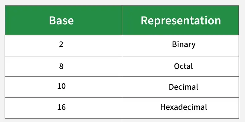
Electronic and digital systems use a variety of number systems, including Decimal, Binary, Hexadecimal, and Octal, which are essential for representing, processing, and storing information in computing and digital electronics.
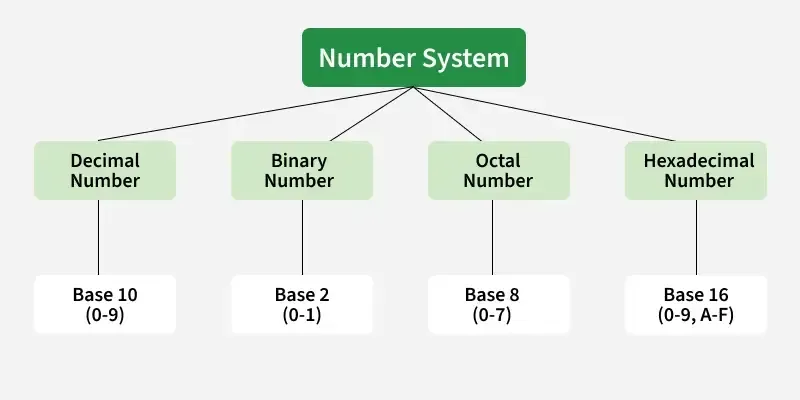
Various Binary System
**1. Decimal (base-10):
- Standard system for everyday calculations, measurements, and financial operations.
- Most familiar number system for humans.
- Used for general data representation and arithmetic operations.
**2. Binary (base-2):
- Core of all digital systems, using only 0 and 1.
- Represents ON and OFF states of electronic circuits.
- Forms the foundation of computer logic, memory storage, and data processing.
**3. Hexadecimal (base-16):
- Simplifies long binary numbers for easier reading and writing.
- Widely used in programming, memory addressing, and digital system design.
- Each hex digit corresponds to four binary bits.
**4. Octal (base-8):
- Condenses binary sequences for simpler representation.
- Less common than hexadecimal but used in older computing systems.
- Useful in certain digital applications for easier conversion and calculation.
**Number System Conversion Methods
A number N in base or radix b can be represented as:
(N)_b = d_n d_{n-1} d_{n-2} \ldots d_1 d_0 . d_{-1} d_{-2} \ldots d_{-m}
- d_{n-1} → Integer part
- d_{−1} to d_{-m} → Fractional part
- d_{n-1} → Most Significant Bit (MSB)
- d_{-m} → Least Significant Bit (LSB)
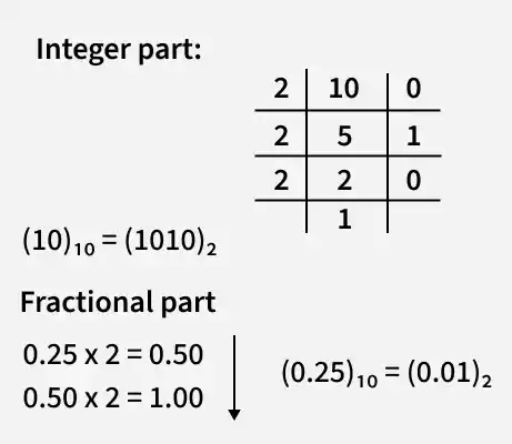
**1. Decimal to Binary
**Steps:
- Divide the decimal number by 2 repeatedly for the integer part.
- Write the remainders from bottom to top to get the binary equivalent.
- For fractional parts, multiply the fraction by 2 repeatedly and record the integer parts.
**Example: (10.25)10
Integer part: 10 ÷ 2 → 1010 Fractional part: 0.25 × 2 = 0.5 → 0, then 0.5 × 2 = 1 → 1 Result: (10.25)10= (1010.01)2
Example
**2. Binary to Decimal
**Steps:
- Multiply each binary digit by 2position starting from the MSB.
- For fractional digits, use negative exponents (2-1,2-2,…2
**Example: (1010.01)2=(10.25)10
1 × 23 + 0 × 22 + 1 × 21 + 0 × 20 + 0 × 2-1 + 1 × 2-2 = 8 + 0 + 2 + 0 + 0 + 0.25 = 10.25 (1010.01)2= (10.25)10
**3. Decimal to Octal
**Steps:
- Divide the decimal number by 8 repeatedly for the integer part.
- Write the remainders from bottom to top.
- For fractional parts, multiply by 8 repeatedly and record the integer parts.
**Example:
(10.25)10
Integer part: 10 ÷ 8 → 12 Fractional part: 0.25 × 8 = 2.0 Result: (10.25)10=(12.2)8
**4. Octal to Decimal
**Steps:
- Multiply each octal digit by 8position8^{\text{position}}8position starting from MSB.
- For fractional digits, use negative exponents (8-1,8-2,… )
**Example:
(12.2) 8
1× 81 + 2 × 80 + 2 × 8-1 = 8 + 2 + 0.25 = 10.25(12.2)8 = (10.25)10
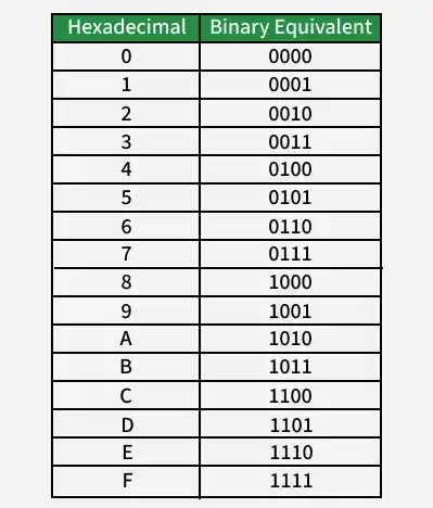
**5. Hexadecimal to Binary
**Steps:
- Convert each hexadecimal digit to its **4-bit binary equivalent.
**Example:
(3A)16 = (00111010)2
**6. Binary to Hexadecimal
**Steps:
- Group the binary digits in **sets of 4 bits starting from the right.
- Add leading zeros if necessary to make full groups.
- Convert each 4-bit group to hexadecimal.
**Example:
(1111011011)2
Add leading zeros → 001111011011 Group: 0011 1101 1011 → 3 D B Result: (1111011011)2 = (3DB)16
**7. Binary to Octal
**Steps:
- Group the binary digits in sets of 3 bits starting from the right.
- Add leading zeros if necessary to complete the groups.
- Convert each 3-bit group to octal.
**Example:
(111101101)2
Group: 111 101 101 → 7 5 5 Result: (111101101)2 = (755)8
**Logic Gates
Logic gates are the basic building blocks of digital circuits. They perform logical operations on one or more binary inputs (0s and 1s) to produce a single binary output. The output depends on the type of gate and the combination of inputs.
**Types of Logic Gates
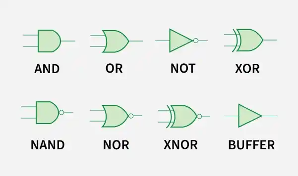
**1. AND Gate (.)
- Performs logical AND operation on inputs.
- Output is 1 only when all inputs are 1.
- Output becomes 0 if any input is 0.
- Symbol “.” is used to represent AND.
**2. OR Gate (+)
- Performs logical OR operation on inputs.
- Output is 1 if at least one input is 1.
- Output is 0 only when all inputs are 0.
- Symbol “+” represents OR.
**3. NOT Gate (')
- Performs logical inversion of the input.
- Output is 1 when input is 0.
- Output is 0 when input is 1.
- Also known as an inverter.
**4. XOR Gate (Exclusive OR)
- Performs exclusive OR operation.
- Output is 1 when inputs are different.
- Output is 0 when inputs are the same.
- For multiple inputs, output is 1 if the number of 1s is odd.
**5. NAND Gate (Not AND)
- Performs NOT of AND operation.
- Output is 0 only when all inputs are 1.
- Output is 1 for all other input combinations.
- It is a universal gate.
**6. NOR Gate (Not OR)
- Performs NOT of OR operation.
- Output is 1 only when all inputs are 0.
- Output is 0 if any input is 1.
- It is a universal gate.
**7. XNOR Gate (Exclusive NOR)
- Performs NOT of XOR operation.
- Output is 1 when inputs are the same.
- Output is 0 when inputs are different.
- For multiple inputs, output is 1 if the number of 1s is even.
**8.Buffer Gate
- Performs no logical operation on input.
- Output is exactly the same as the input.
- Used to strengthen or amplify signals.
- Helps drive circuits without signal degradation.
**Universal Logic Gates
- NAND and NOR gates are universal because any digital circuit can be implemented using only these gates.

Minimization of Boolean Function
Minimization of a Boolean function involves reducing the number of terms, literals, and gates required to represent a Boolean expression. The goal is to create a simpler and more efficient digital circuit without altering its functionality and the minimization techniques are given below:
**1. Algebraic Simplification
Algebraic simplification uses Boolean algebra laws to reduce expressions.
**Example: F(A,B) = AB + A ⇒ F(A,B) = A
**2. Karnaugh Map (K-Map) Method
The Karnaugh Map is a visual technique used to simplify Boolean expressions with 2, 3, 4, or more variables.
Steps:
- Construct a K-Map with cells representing the truth table outputs.
- Group adjacent 1s into powers of two (1, 2, 4, 8, etc.).
- Derive the simplified Boolean expression by writing terms for each group.
Representation of Boolean Functions
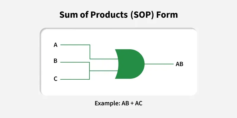
**1. Sum of Products (SOP) Form
- Written as a sum (OR) of product (AND) terms.
- Derived directly from truth table rows where output = 1.
- Uses AND gates followed by an OR gate in implementation.
- Represented using Σ (sigma) notation of minterms.
- Commonly used in combinational circuit design.
- Easy to simplify using K-Maps and Boolean algebra.
**Example:
Y = AB+AC
𝑓(𝐴,𝐵,𝐶) = Σ𝑚(1,3,5)
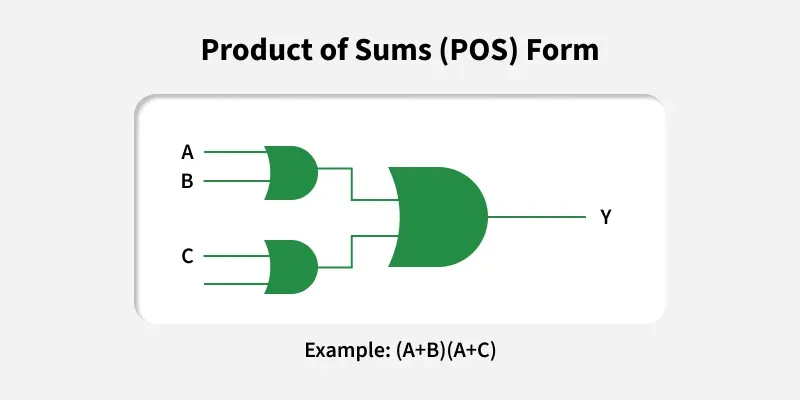
**2. Product of Sums (POS) Form
- Written as a product (AND) of sum (OR) terms.
- Derived from truth table rows where output = 0.
- Implemented using OR gates followed by an AND gate.
- Represented using Π (pi) notation of maxterms.
- Commonly used when output conditions for logic 0 are specified.
- Can be simplified using K-Maps and Boolean algebra.
**Example:
Y = (A+B)(A+C)
f(A,B,C) = ΠM(0,2,4)
Read more about Instruction Format, Here.
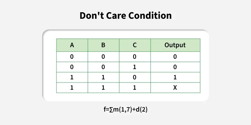
**3. Don’t Care Condition
- Unused or irrelevant output combinations.
- Denoted by X or d.
- Can be treated as 1 or 0 for simplification.
**Example:
f = Σm(1,3,7) + d(2)
Read more about Instruction Format, Here.
Important Laws in Boolean Algebra
| **Law Name | **Statement / Rule | **Example |
|---|---|---|
| **De Morgan’s Laws | Complement of AND is OR of complements | ((A·B)’ = A’ + B’) |
| Complement of OR is AND of complements | ((A + B)’ = A’·B’) | |
| **Absorption Law | Removes redundant terms | (A + AB = A) |
| (A(A + B) = A) | ||
| **Domination Law | OR with 1 gives 1 | (A + 1 = 1) |
| (Zero & One Law) | AND with 0 gives 0 | (A·0 = 0) |
| **Consensus Law | Eliminates unnecessary terms | (AB + A'C + BC = AB + A'C) |
| (POS form) | ((A + B)(A' + C)(B + C) = (A + B)(A' + C)) | |
| **Duality Theorem | Swap AND ↔ OR, 0 ↔ 1 | Dual of (A + BC) is (A(B + C)) |
Combinational Circuits
Combinational circuits are a type of digital circuit in which the output depends only on the current inputs, not on past inputs or previous states. These circuits are built using logic gates like AND, OR, NOT, NAND, NOR, XOR, and XNOR.
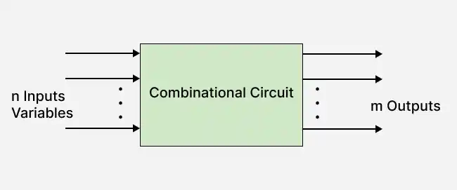
Block Diagram of Combinational Circuit
Basic Examples of Combinational Circuits are:
**1. Adders: The most basic arithmetic operation is the addition of two binary digits. A combinational circuit that performs the addition of two 1-bit numbers is called as half adder, and the logic circuit that adds three 1-bit numbers is called as full adder.
- **Half Adder: Adds two single-bit binary numbers (A and B).
**Inputs: A, B
**Outputs: Sum (S), Carry (C).
Logic:
S=A⊕B
C=A⋅B
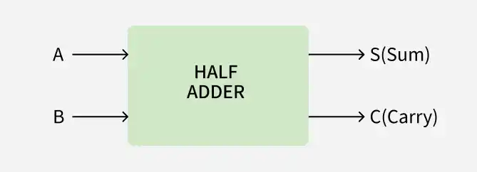
Half Adder
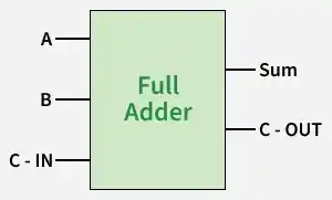
- **Full Adder: Adds three single-bit numbers (A, B, and Carry-in).
A **Full Adder adds three inputs: two operands (**A, B) and a carry-in (**Cin) and produces a **Sum (S) and **Carry-out (Cout).
- **Sum (S) = A ⊕ B ⊕ Cin
- **Carry-out (Cout) = (A · B) + (B · Cin) + (A · Cin)
**2. Subtractors:
- **Half Subtractor: A half subtractor is a combinational logic circuit, which performs the subtraction of two 1-bit numbers. Half Subtractor subtracts one binary digit from another to produce a DIFFERENCE output and a BORROW output.
**Outputs: Difference, Borrow. - A Half Subtractor subtracts two bits (A - B) and gives a Difference (D) and Borrow (Bout).
Difference (D) = A ⊕ B
Borrow (Bout) = A' · B
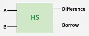
Half Subtractor
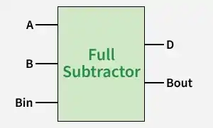
- **Full Subtractor: Subtracts three single-bit numbers, including Borrow-in.
A Full Subtractor subtracts two operands (A, B) and a Borrow-in (Bin), producing a Difference (D) and Borrow-out (Bout).
- Difference (D) = A ⊕ B ⊕ Bin
- Borrow-out (Bout) = A' · (B ⊕ Bin) + (B · Bin)
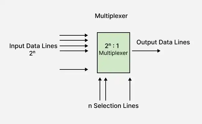
**3. Multiplexers (MUX): A multiplexer is a combinational circuit that has many data inputs and a single output, depending on control or select inputs. For N input lines, log2(N) selection lines are required, or equivalently, for 2n input lines, n selection lines are needed. Multiplexers are also known as “N-to-1 selectors,” parallel-to-serial converters, many-to-one circuits, and universal logic circuits.
Multiplexer
**Implementation of Higher-Order MUX Using Lower-Order MUX
A higher-order multiplexer (MUX) can be built using multiple lower-order MUXes to handle more input lines. This is done by breaking the selection process into smaller steps using additional MUXes.
For example, an **8:1 MUX can be implemented using **two 4:1 MUXes and **one 2:1 MUX:
- The two 4:1 MUXes take inputs and provide two outputs.
- The 2:1 MUX selects one of these outputs based on the highest selection bit.
This method reduces complexity and allows modular circuit design.
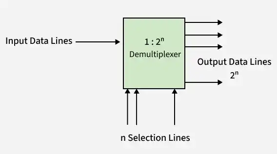
**4. Demultiplexers (DEMUX): The DEMUX is a digital information processor. It takes input from one source and also converts the data to transmit towards various sources. The demultiplexer has one data input line. The demultiplexer has several control lines (also known as select lines). These lines determine to which output the input data should be sent. The number of control lines determines the number of output lines.
**5. Encoders: An Encoder is a combinational circuit that performs the reverse operation of a Decoder. It has a maximum of 2^n input lines and ‘n’ output lines, hence it encodes the information from 2^n inputs into an n-bit code. It will produce a binary code equivalent to the input, which is active High. Therefore, the encoder encodes 2^n input lines with ‘n’ bits.
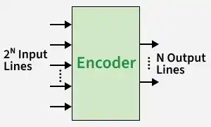
**Priority Encoder
A priority encoder is a digital circuit that converts multiple input lines into a binary code based on priority. If multiple inputs are active, the highest-priority input (the one with the highest index) is encoded in the output.
**Key Features:
- Assigns priority to inputs when more than one is active.
- Ignores lower-priority inputs when a higher-priority input is present.
- Commonly used in interrupt controllers and other selection-based applications.
**6. Decoders: A decoder is a combinational circuit that converts an n-bit binary input data into 2n output lines, such that each output line will be activated for only one of the possible combinations of inputs. Decoders are usually represented as n-to-2 n line decoders, where n is the number of input lines and 2n is the number of maximum possible output lines.
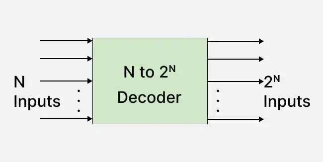
Decoder
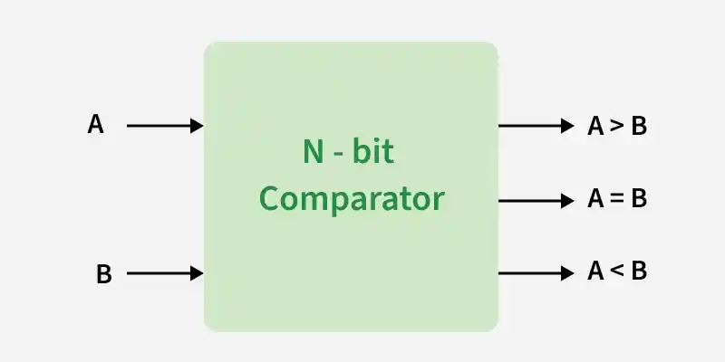
**7. Comparators: The comparator is a combinational logic circuit. It compares the magnitude of two n-bit numbers and provides the relative result as the output. Let A and B are the two n-bit inputs. The comparator has three outputs namely A > B, A = B and A < B. Depending upon the result of comparison, one of these outputs will go high.
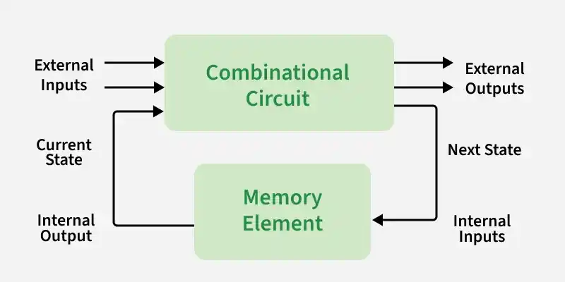
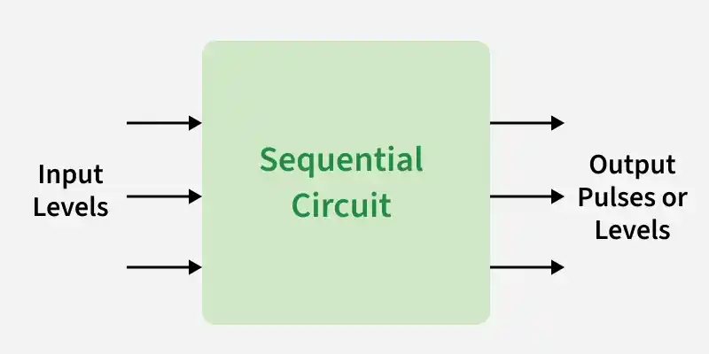
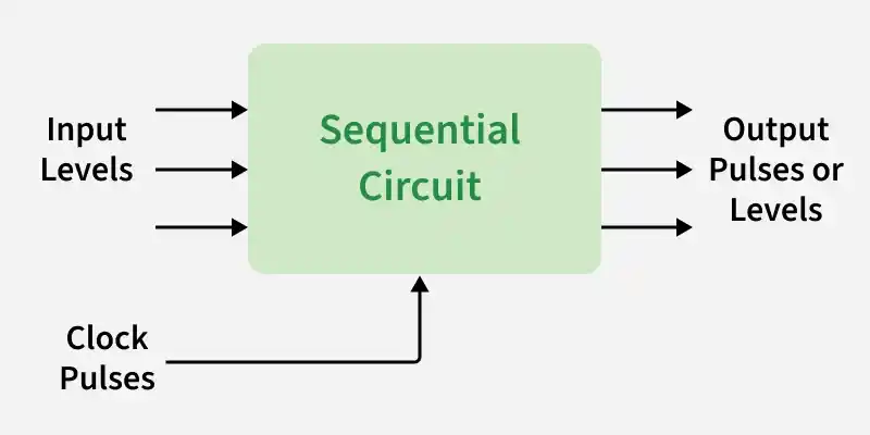
Sequential Logic Circuits
Sequential circuits are digital circuits that store and use previous state information to determine their next state. They are commonly used in digital systems to implement state machines, timers, counters, and memory elements and are essential components in digital systems design.
Sequential Circuit
**Types of Sequential Circuits
**1. Asynchronous Sequential Circuits
Asynchronous sequential circuits operate without a clock signal and respond directly to changes in input signals. The circuit state updates as soon as an input changes, resulting in very fast operation. However, the absence of clock control makes timing difficult, which can affect stability.
- Do not require a clock signal for operation
- State changes are triggered directly by input variations
- Very fast response since there is no clock delay
- Timing control is difficult due to lack of synchronization
- Design and analysis are complex
- Lower stability and reliability in large systems
Asynchronous Sequential Circuits
**2. Synchronous Sequential Circuits
Synchronous sequential circuits operate using a clock signal that controls when state changes occur. Inputs are evaluated only at clock pulses, ensuring predictable and controlled operation. Although this introduces a delay, these circuits are easy to design and highly reliable, making them widely used.
- Operate with a clock signal for synchronization
- State changes occur only at clock pulse instants
- Predictable operation due to controlled timing
- Slight delay caused by waiting for clock pulses
- Easier to design and test
- High stability and reliability
Flip-Flops
The flip-flop is a circuit that maintains a state until directed by input to change the state. A basic flip-flop can be constructed using four-NAND or four-NOR gates. Flip-flop is popularly known as the basic digital memory circuit. It has its two states as logic 1(High) and logic 0(low) states. A flip flop is a sequential circuit which consist of single binary state of information or data.
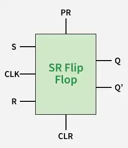
**1. S-R Flip-Flop (Set-Reset): S-R Flip-Flop stores one bit of data and can be set or reset using S and R inputs.
Preset and Clear inputs are used to fix the initial state of the flip-flop.
- Stores a single bit.
- Without control, the output is **uncertain when powered on.
- **Preset (PR): Forces Q = 1
- **Clear (CLR): Forces Q = 0
- Used when a known initial state is needed.
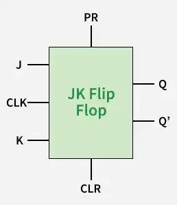
**2. J-K Flip-Flop: J-K Flip-Flop stores a single bit and can set, reset, or toggle depending on J and K inputs.
It eliminates the undefined state problem present in S-R flip-flop.
Improved S-R flip-flop; avoids invalid state.
Inputs: J, K, Clock, Preset, Clear
Behavior:
- J=0, K=0 → No change
- J=0, K=1 → Reset (Q=0)
- J=1, K=0 → Set (Q=1)
- J=1, K=1 → Toggle Q
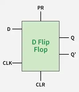
**3. D Flip-Flop: D Flip-Flop captures and stores the input value D at the clock edge.
It provides Q and Q’ outputs without any invalid or undefined state.
- Stores the value of the data input (D) at the clock edge.
- Inputs: D, Clock
- Outputs: Q, Q’ (complement)
- Q takes the value of D when the clock triggers.
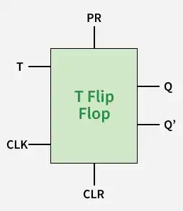
**4. T Flip-Flop: T Flip-Flop toggles its output on each clock pulse when T = 1 and holds state when T = 0.
It can be implemented using a J-K flip-flop by connecting J and K together.
- Toggles its output when T = 1.
- Inputs: T, Clock
- Outputs: Q, Q’ (complement)
- T=0 → Q does not change, T=1 → Q toggles.
- Used in counters and frequency dividers.
| Flip-Flop | Inputs | Output Behavior | Use |
|---|---|---|---|
| S-R | S, R, PR, CLR | Q set or reset | Initial state control |
| J-K | J, K, CLK | Set, reset, toggle | Versatile, no invalid state |
| D | D, CLK | Q = D | Store data |
| T | T, CLK | Q toggles | Counters |